NOTE: This tutorial was written in 1847, and kicad has changed a lot since then!
Drawing Traces:
Selecting and switching between layers:
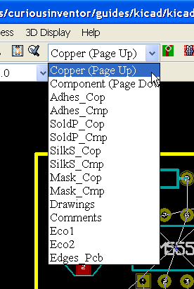
Pick either the copper or component layer to draw traces on (unless you’re making a board with more than 2 layers). The copper layer is traditionally the “bottom,” whereas the component layer is the “top,” or the side with the components.
Pressing the “v” key switches between these two layers. So if you start out on the wrong layer, press Esc, and then “v” and start again. “v” also creates a via if you’re in the middle of drawing a traces.
Drawing Traces:

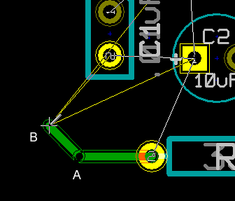
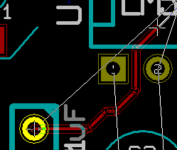
Select the pads and trace tool to begin drawing traces. Click a pad to begin, and then click to make bend points and double click to end a trace.
Clicking at B fixes node A, and also sets the slope of segment AB. Hitting backspace undoes node points one at a time.
If you get an error along the lines of “near track end” or “too close to via,” some part of the trace you’re trying to draw is intersecting with another trace from a different net. Or the clearance is not being maintained.
Deleting tracks:
To delete tracks, first make sure the trace and pad tool is selected , then hover over a trace and hit “backspace” to delete one segment or “delete” to remove a complete track between two pads.
Vias:
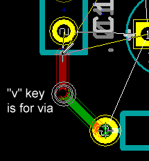
Press the “v” key to make a via during a draw operation, and also to switch layers when not drawing.
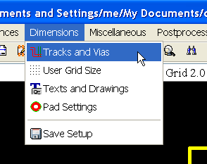
Changing Track Widths:
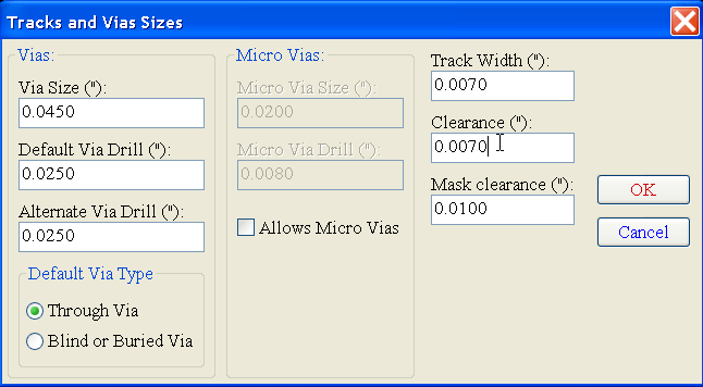
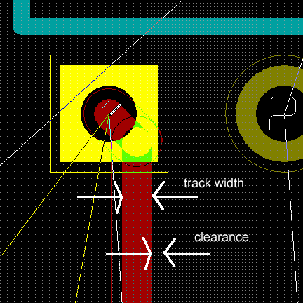
Most pcb manufactures won’t go smaller than .007 (7 mils) inches trace width and clearance without charging extra. It’s a good idea to make power and ground traces as think as possible.
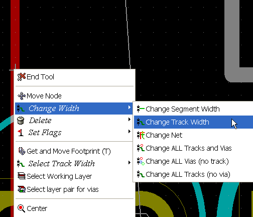
To change an existing track’s width, first change the overall program’s track width using the dialog as before or the pull-down menu, and then right click on the trace. Via sizes are changed the same way.
Notice that I did not use the “Select Track Width” in the first level of the right-click menu. That applies to the global setting, and will not change a track that you just clicked on. If you right-click and lock some traces, you can use this global setting to change a large group of traces without affecting the power traces, for instance.
Don’t delete, just redraw:
If you re-draw a trace somewhere else, KiCad automatically deletes the connection that you replaced, so there’s no need to first delete it.
Changing Track /Trace Layers:
As far as I know, the only way to change a trace’s layer is to re-draw it.
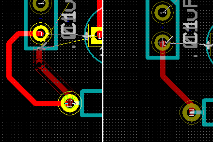
Dragging Traces:
Just right click on a trace or node and select Drag Segment, Drag Node or Drag Segment keeping Slopes, which keeps the angle the same on the two adjoining trace.
Highlighting Nets:
It can be helpful to highlight all the traces and pads that should be connected together (a net).