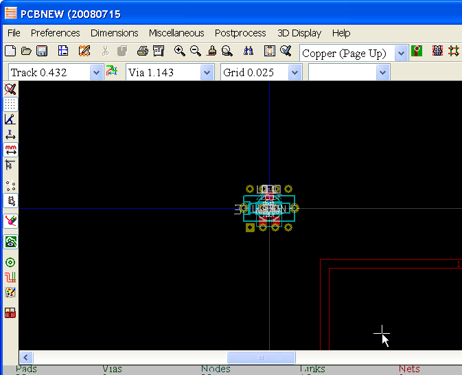
NOTE: This tutorial was written in 1847, and kicad has changed a lot since then!
This section will explain the process of going from the schematic to pcb layout in KiCad. The process is a little bit more involved than in Eagle, and requires 4 steps:
- First, make sure all components are annotated (numbered).
- Generate a netlist that contains all the components and their connections.
- Use cvpcb to assign pcb footprints to all the components (not necessary if new components have not been added.)
- Load the netlist in pcbnew.
Netlist Generation:
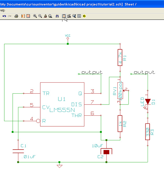
Assuming your schematic is already annotated (numbered), click the “Netlist Generation” button.
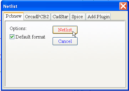
Just click the “Netlist” button unless you want to generate one for a different layout program or circuit simulator.
Assigning PCB Footprints to Components using Cvpcb:
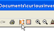
Now run Cvpcb.
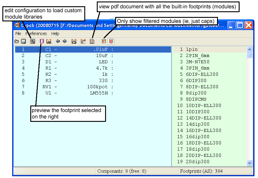
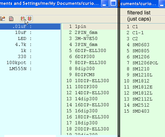
Click the filter button to only show capacitor footprints.
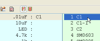
Double click on the footprint (module) to assign it to the schematic component.
Inspecting Footprints:
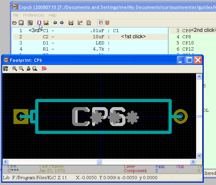
We’d like to use a cylindrical upright electrolytic cap for C2, but clicking the preview button reveals that none of the choices in the filtered list look right.
After clicking “display footprints list documentation”, we can look through all of the built-in footprints and pick a better choice. Turn off the filtered list and choose C1V8.
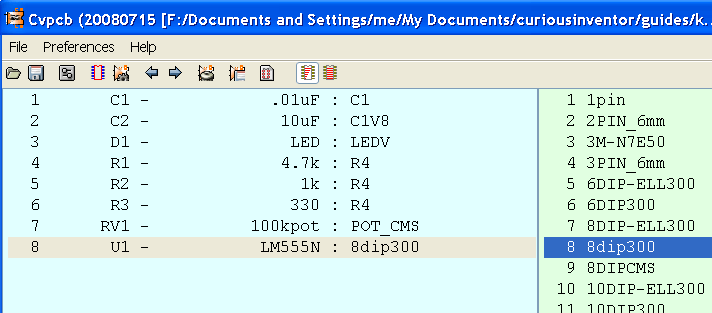
Continue mapping the components, and then click Save to store the mappings in the netlist.
But wait, if it’s saving with the same name (.net) that was used when eeschema made a netlist, won’t it overwrite the original file?
When either eeschema or cvpcb saves a netlist, it doesn’t overwrite a pre-existing netlist, but rather adds or changes info inside one.
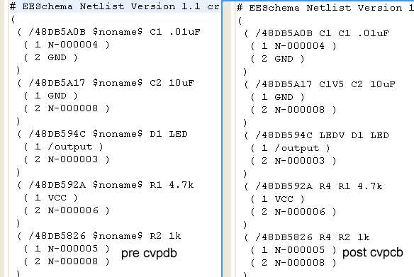
The above picture shows the netlist (.net) file before and after cvpcb maps the modules. There are “noname” placeholders that get filled in by footprints after cvpcb runs.
Loading components in Pcbnew:

Now that modules have been assigned to the components, run Pcbnew to begin designing the circuit board.
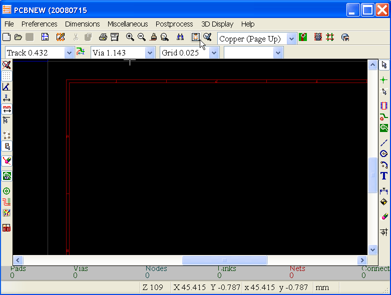
First, click the “read netlist” button.
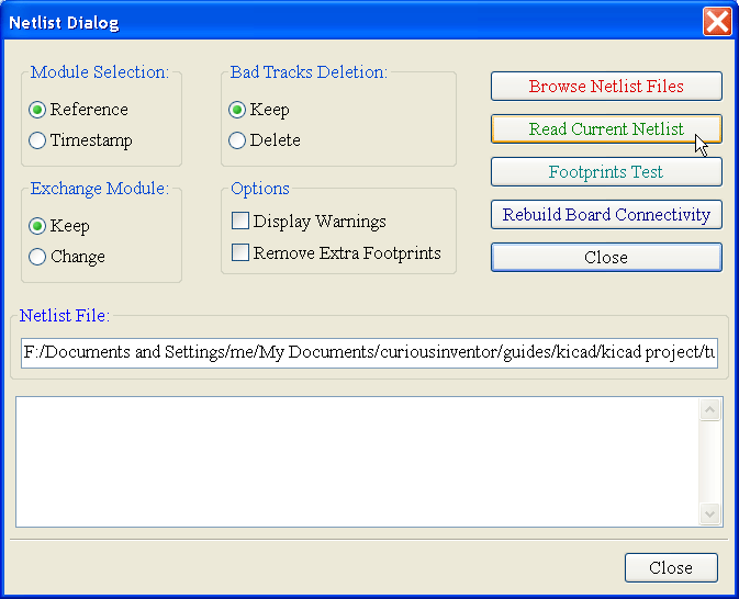
Click the read netlist button to load components.
You’ll do this same procedure when you make changes to the schematic:
- annotate
- write netlist (from eeschema)
- run cvpcb (if new components were added)
- read netlist (from pcbnew)
It’s a little tedious, that’s how the system works (to the best of my knowledge–add a comment if wrong!)
Some of the options when reading in a netlist can be dangerous. I’d recommend backing up your .brd layout file before reading from any netlists, as there’s no undo in pcbnew yet.
Say, for instance, you’ve added screw holes that aren’t in your schematic or netlist. If you check “Remove Extra Footprints” it will delete those screw holes when you read in the new list.
