Designing PCBs in Kicad and PcbNew:

NOTE: This tutorial was written in 1847, and kicad has changed a lot since then!

Contents:

Arrange Components:

Grid First!

adjust the grid size in kicad adjust the grid size in kicad

You’ll probably want to adjust the grid size before moving anything. The pull down contains the user grid size as well as several sizes listed in mils (thousandths of an inch).

Group Move:

move a group of components by selecting

When you first read a net-list, all the components will come in on top of each other.

Start off by moving the whole pile of components by drawing a selection rectangle around them and then click in the middle of the sheet.

Auto Un-Piling

turn on auto-move moderight click and select move all to unpile the components

Pcbnew will automatically unpile the components. First, enable the automatic mover by clicking the “Mode Module” button in the top toolbar. Then right click and select “Move All Modules”. Pcbnew also has an “auto placer,” which is different in that it tries to minimize the length of the connections between the modules (the ratsnest). You can fix components to prevent them from being moved by either command.

General Moving and Rotating–use keyboard shortcuts:

move components by pressing m or r

Continue moving components around by hovering the mouse pointer over them, and then pressing “m” or “r” to move or rotate.

Rats Nest (show rubber bands where all connections should be):

show the rats nest

<-Back                                                                                       Next->

Designing PCBs in Kicad and PcbNew: Drawing the Board Outline

NOTE: This tutorial was written in 1847, and kicad has changed a lot since then!

Drawing the Board Outline:

edges.gif

drawing a board outline with the polyline tool

First select the edges layer, and then draw an outline using the line tool. Double click to finish the poly-line.

Tip: Drawing set lengths and measuring:

measure by hitting space bar to zero the relative position readout.

Hit space bar at the start of a line to zero out the relative coordinates at the bottom of the screen. The coordinates will then measure from that point.


<-Back                                                                                       Next->

designing PCBs in Kicad and PcbNew: Drawing Traces

NOTE: This tutorial was written in 1847, and kicad has changed a lot since then!

Drawing Traces:

Selecting and switching between layers:

picking the copper layer in kicad

Pick either the copper or component layer to draw traces on (unless you’re making a board with more than 2 layers). The copper layer is traditionally the “bottom,” whereas the component layer is the “top,” or the side with the components.

Pressing the “v” key switches between these two layers. So if you start out on the wrong layer, press Esc, and then “v” and start again. “v” also creates a via if you’re in the middle of drawing a traces.

Drawing Traces:

select the trace tool click to set bend points when drawing traces in kicad

Select the pads and trace tool to begin drawing traces. Click a pad to begin, and then click to make bend points and double click to end a trace.

Clicking at B fixes node A, and also sets the slope of segment AB. Hitting backspace undoes node points one at a time.

If you get an error along the lines of “near track end” or “too close to via,” some part of the trace you’re trying to draw is intersecting with another trace from a different net. Or the clearance is not being maintained.

Deleting tracks:

deleting tracks in kicad

To delete tracks, first make sure the trace and pad tool is selected select the trace tool , then hover over a trace and hit “backspace” to delete one segment or “delete” to remove a complete track between two pads.

Vias:

press v to make a via in kicad

Press the “v” key to make a via during a draw operation, and also to switch layers when not drawing.

Changing Track Widths:

changing track sizes in kicad changing track sizes in kicad

Most pcb manufactures won’t go smaller than .007 (7 mils) inches trace width and clearance without charging extra. It’s a good idea to make power and ground traces as think as possible.

7 mil trace in kicad track clearance markings while drawingchanging track width

To change an existing track’s width, first change the overall program’s track width using the dialog as before or the pull-down menu, and then right click on the trace. Via sizes are changed the same way.

Notice that I did not use the “Select Track Width” in the first level of the right-click menu. That applies to the global setting, and will not change a track that you just clicked on. If you right-click and lock some traces, you can use this global setting to change a large group of traces without affecting the power traces, for instance.

Don’t delete, just redraw:

redo traces by drawing somewhere else

If you re-draw a trace somewhere else, KiCad automatically deletes the connection that you replaced, so there’s no need to first delete it.

Changing Track /Trace Layers:

As far as I know, the only way to change a trace’s layer is to re-draw it.

Dragging Traces:

Just right click on a trace or node and select Drag Segment, Drag Node or Drag Segment keeping Slopes, which keeps the angle the same on the two adjoining trace.

Highlighting Nets:

highlighting nets

It can be helpful to highlight all the traces and pads that should be connected together (a net).


<-Back                                                                                      Next->

designing PCBs in Kicad and PcbNew: Undo and Adding Screw Holes

NOTE: This tutorial was written in 1847, and kicad has changed a lot since then!

UnDo… not yet, but there is an UnDelete:

undelete in kicad's pcbnew

It’s pretty easy to accidentally delete an entire track, so this is actually very helpful. Unfortunately, there is no general purpose undo that I know about.

Adding Screw Holes:

One of the quirks of KiCad is that you can’t just drill a hole, you need to make a one-pad component that has the right sized hole for your screw. The module called “1PIN” is the right size for a 4-40 screw.

adding new modules inside pcbnew

Click the “Add Modules” button.

type in the module name for 1PIN

Type in 1PIN and click OK or click “List All” to browse by library.

place the screw hole and repeat for the other 3 corners

Place the screw hole and repeat for the other 3 corners.


<-Back                                                                                       Next->

Designing PCBs in Kicad and PcbNew: Changing Parts

NOTE: This tutorial was written in 1847, and kicad has changed a lot since then!

Changing Parts:

If you want to delete, add or functionally change a component, it’s best to change the schematic and repeat the entire process again:

  • Make changes in eeschema, re-annotating the components if necessary (putting numbers in for R?, C?, etc.)
  • Save netlist in eeschema (schematic editor)
  • Run Cvpcb and assign a footprints / modules to the new components
  • Read the netlist again in Pcbnew (backup the .brd first!)

If you’re just changing the footprint of a module, for instance, going from a 1/4W resistor to a larger 1/2W, you can make the changes just in Pcbnew (explained below).

Deleting, Adding or Making other Major Changes:

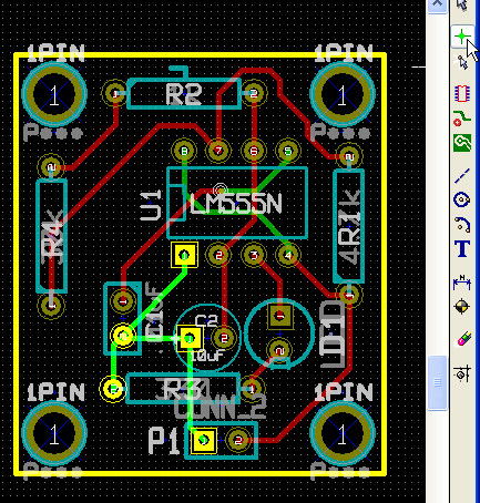
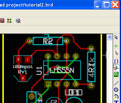
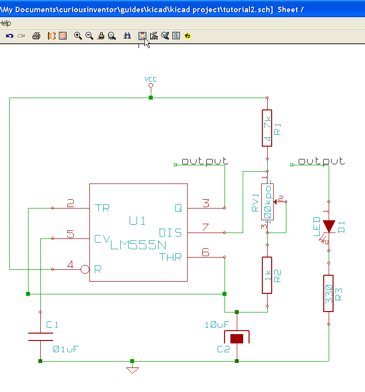
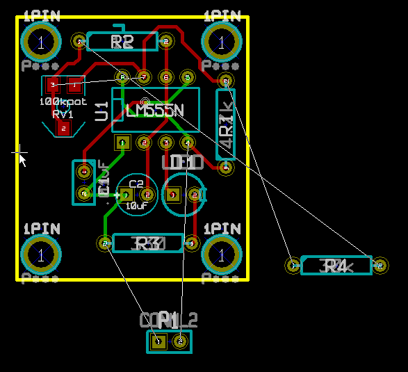
As just stated above, make the changes in the schematic using eeschema. We’ll add a 2-pin header for power, and replace the pot with a fixed resistor.

adding a 2 pin connector in kicad / eeschema2 new parts in kicad

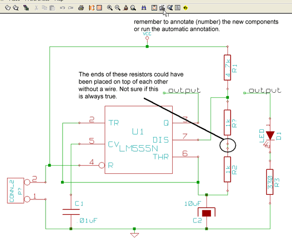
Add the 2-pin connector, wire it up, delete the pot and re-wire a resistor in its place.

generating a netlist in kicad

Again, save the netlist, and then open Cvpcb.

cvpcb kicad

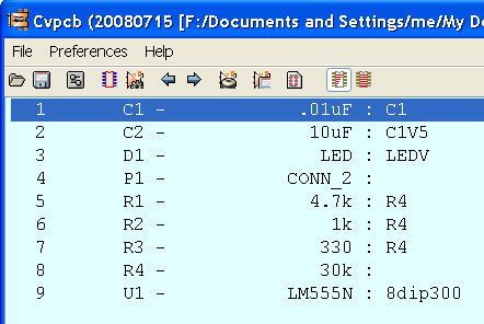
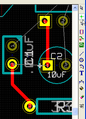
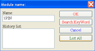
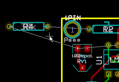
The new netlist should have two blanks in it now. Assign the module SIL-2 to the CONN_2 connector and another R4 to the resistor. Save the netlist again.

read netlist in pcbnew

Open Pcbnew and click the “Read netlist” button.

click the read net list button to load componentsclick the read net list button to load new components

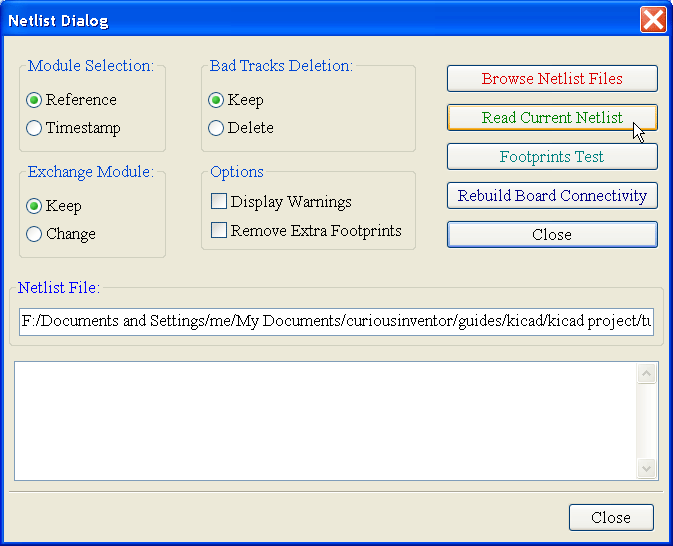
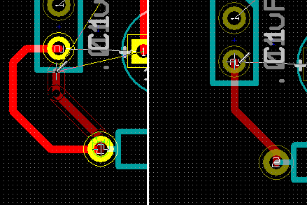
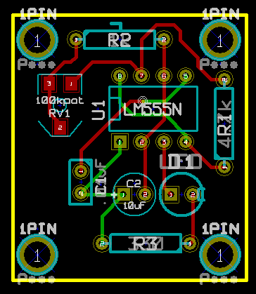
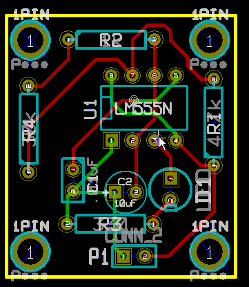
If you just click “Read Current Netlist” in the dialog without changing any options, it adds the two new components, but doesn’t delete the old ones and their stale tracks.

click the read net list button to load new components 

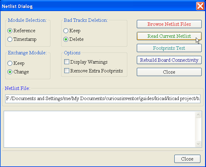
Selecting “Change” and “Delete” under “Exchange Module” and “Bad Tracks Deletion” gets rid of some of the bad traces, but still doesn’t delete module RV1. Had RV1 been labeled R4 before, it would have indeed deleted the module and replaced it with the new R4.

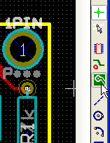
But since RV1 has a different name, the only way to get rid of it is to manually delete it or select “Remove Extra Footprints” under “options.” We can’t select that option, however, because that would delete any modules that are not in the netlist (or the .cmp file), which includes our screw holes.

555 timer circuit

Changing Just a Module, and Not the Circuit:

This can be done solely in Pcbnew without going back into Cvpcb or Eeschema.

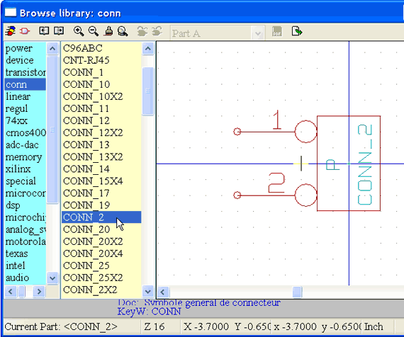
You can either swap out a module for a different one from the library, or actually edit the silk screen and pin layout.

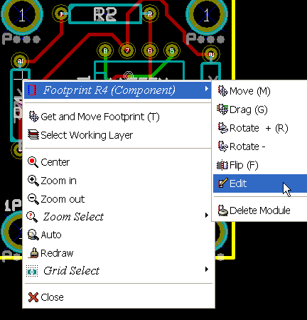
First, right click on a component and edit the footprint.

Then click “Change Module”.

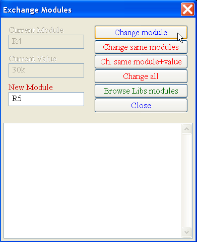
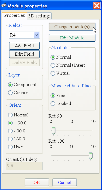
Type in “R5” or Browse to find a new module, then click “Change Module”.

A new, longer resistor footprint should be in place. Although the netlist didn’t change, another file also used to keep track of modules has: the .cmp file. Next time you run Cvpcb, it will already show a new R5 module mapped to R4. The naming convention is extremely confusing here–R4 is a component label, and R5 is actually a foot print name.

By clicking “Edit Module” in the above Module Properties dialog, you could open up the module editor and actually change the shape and pin arrangement of the footprint. The resulting module would be saved in the .brd file, and not a library (I think).


<-Back                                                                                       Next->

Designing PCBs in Kicad and PcbNew: Adding Copper Fills/Zones

NOTE: This tutorial was written in 1847, and kicad has changed a lot since then!

Adding Copper Fills / Zones:

In KiCad, filling an area with copper does not create any connections, so the first step is to finish drawing all the traces as normal.

Use the highlight tool to highlight the net for which you will be creating a zone(GND in our case).


Select the zone tool and click somewhere to start the outline (this will bring up the zone dialog).

Select the NET, layer and pad options, which is how the zone will connect to pads that are part of the net. If you choose “include pads,” the copper fill will completely connect to the pad, which will make it very hard to solder as a large amount of heat will be drawn away. The “thermal” connection option makes several fingers that connect the pad to the fill area, thus reducing the thermal connection so it’s easier to bring the pad up to temperature during soldering.

Also, the zones are filled with individual trace lines, so choosing a grid that’s big will create large gaps, and choosing a grid that’s too small will create extremely large files. The KiCad author recommends .01″

Draw the Zone:

Adding Cutouts:

Right click with the zone tool on an existing zone outline.

Filling the Zone:

Just right click in the boundary and select fill.


<-Back                                                                                       Next->

Designing PCBs in Kicad and PcbNew: Making Gerbers (files needed by the manufacturer)

NOTE: This tutorial was written in 1847, and kicad has changed a lot since then!

Making Gerbers (files needed by the manufacturer):

making gerber with plot from the file menu

For a 2 layer board, you would commonly want files that represent the metal on the top and bottom (component and copper, respectively), top and bottom solder mask (the green stuff), the top silk screen, the board outline (edges), and a drill file (click “Create Drill File” in addition to “Plot”).

<-Back                                                                                       Next->

About

CuriousInventor launched in late 2006 (pre-arduino era!) as a place to enable hobbyists, students, and musicians to create their own technology. We sold open-source kits and tools, and offered numerous guides & videos on things like soldering, metal working, screws, electronics, and more. 

The store is now mostly empty, but we’ve kept the product pages and guides up since they have useful information. Many of our guides and videos still rank on the first page of google searches and have been seen millions of times. Content on this site and the CuriousInventor YouTube channel produced by Scott Driscoll.

Top Videos