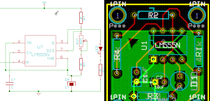
NOTE: This tutorial was written in 1847, and kicad has changed a lot since then!
Intro:

This set of tutorials will cover some essentials to designing circuits and pcb layouts using kicad (link goes to author’s site + download), an open-source tool for circuit (board) design that’s free and has no restrictions on number of layers or size (like Eagle). We’ll focus more on the unintuitive things as well as tips & tricks rather than re-write the manual.
Contents:
- KiCad sub-program overview, and how to make Schematics
- Going from Schematic to PCB Layout, Using Cvpcb This process is more involved than in Eagle, and requires the creation of a netlist, and a separate program (Cvpcb) that assigns footprints to schematic symbols, which are both stored in different libraries.
- Creating PCB Layouts, Using Pcbnew
- Arrange Components
- Drawing the Board Outline
- Drawing Traces
- UnDo… not yet, but there is an UnDelete and Adding Screw Hole
- Changing Parts
- Adding Copper Filles / Zones
- Making Gerbers (files needed by the manufacturer)
- Creating New Components, both Schematic Symbols and Footprints (Modules) There are two different editors and two different types of libraries for schematic symbols and pcb footprints.
