Intro: There are all sorts of guides that explain how to interface a PS2 controller already out there. The goal here is to consolidate the information and make it as fast as possible to get up and running. Please let us know about mistakes!
Update: Check out the arduino ps2 library that Bill Porter helped polish.
Contents:
- Hardware Interface / Wiring Connections
- Software Protocol
- Low Level: how individual bytes are transfered
- high level: packet descriptions / protocol
- Button Mappings for PS2 Dual Shock controller and Guitar Hero controller.
- Complete Command listing and explanations.
- Example Commands necessary to read all analog (joysticks and pressures) and control motors
- Recorded Command and Response between real PlayStation and Controller during first connect
- MPLAB projects (c code) for PIC18f4550 to control a PS2. You’ll need a programmer (PICKIT2) and www.microchip.com ‘s free IDE, MPLAB.
Hardware Interface / Wiring Connections:
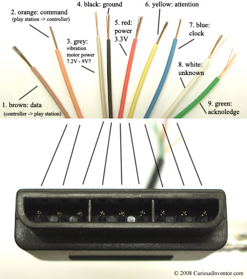
Wire Colors and Functionality: There are 9 wires, 6 wires are needed at a minimum to talk to the controller: (clock, data, command, power & ground, attention). To operate vibration motors, motor_power is also needed.
- Brown – Data: Controller -> PlayStation. This is an open collector output and requires a pull-up resistor (1 to 10k, maybe more). (A pull-up resistor is needed because the controller can only connect this line to ground; it can’t actually put voltage on the line).
- Orange – Command: PlayStation -> Controller.
- Grey – Vibration Motors Power: 6-9V? With no controller connected, this meausures about 7.9V, with a controller, 7.6V, most websites say this is 9V (except playstation.txt -> 7.6V), although it will still drive the motors down around 4V, although somewhat slower. When the motors are first engaged, almost 500mA is drawn on this line, and at steady state full power, ~300mA is drawn.
- Black – Ground
- Red – Power: Many sites label this as 5V, and while this may be true for Play Station 1 controllers, we found several wireless brands that would only work at 3.3V. Every controller tested worked at 3.3V, and the actual voltage measured on a live Playstation talking to a controller was 3.4V. McCubbin says that any official Sony controller should work from 3-5V. Most sites say there is a 750mA fuse for both controllers and memory cards, although this may only apply to PS1’s since 4 dual shock controllers could exceed that easily.
- Yellow – Attention: This line must be pulled low before each group of bytes is sent / received, and then set high again afterwards. In our testing, it wasn’t sufficient to tie this permanently low–it had to be driven down and up around each set. Digitan considers this a “Chip Select” or “Slave Select” line that is used to address different controllers on the same bus.
- Blue – Clock: 500kH/z, normally high on. The communication appears to be SPI bus. We’ve gotten it to work from less than 100kHz up through 500kHz (500k bits / second, not counting delays between bytes and packets). When the guitar hero controller is connected, the clock rate is 250kHz, which is also the rate the playstation 1 uses.
- White – Unknown
- Green – Acknowledge: This normally high line drops low about 12us after each byte for half a clock cycle, but not after the last bit in a set. This is a open collector output and requires a pull-up resistor (1 to 10k, maybe more). playstation.txt says that the playstation will consider the controller missing if the ack signal (> 2us) doesn’t come within 100us.
Low-Level – How Bytes and Packets are Transferred:
The play station sends a byte at the same time as it receives one (full duplex) via serial communication. The following pictures show actual signals between a playstation and guitar hero controller configured in analog mode (wammy bar sends back 7-bit value (0x7f – 0x00)).
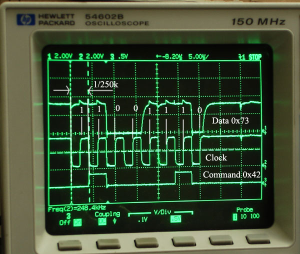
The clock is held high until a byte is to be sent. It then drops low (active low) to start 8 cylces during which data is simultaneously sent and received. When the clock edge drops low, the values on the line start to change. When the clock goes from low to high, value are actually read. Bytes are transferred LSB (least significant bit) first, so the bits on the left (earlier in time) are less significant.
 |
 |
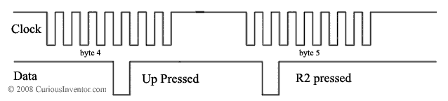
Scope shots showing the acknowledge and attention lines.
High-level: Packet structure, Command and Data Meanings:
Much of this section is sourced from Dowty’s consolidation and home-brew port sniffer and emulator.
Packets have a three byte header followed by an additional 2, 6 or 18 bytes of additional command and controller data (like button states, vibration motor commands, button pressures, etc.).
An example exchange that from a dual shock controller when first plugged in:
Controller defaults to digital mode and only transmits the on / off status of the buttons in the 4th and 5th byte. No joystick data, pressure or vibration control capabilities.
(no buttons pressed)
| byte # | 1 | 2 | 3 | 4 | 5 |
| Command | 0x01 | 0x42 | 0x00 | 0x00 | 0x00 |
| Data | 0xFF | 0x41 | 0x5A | 0xFF | 0xFF |
Explanation:
— Header: (always the first three bytes)
| byte # | source / type |
example value |
explanation |
| 1st byte | Command | 0x01 | New packets always start with 0x01 … 0x81 for memory card? |
| Data | 0xFF | always 0xFF | |
| 2nd byte | Command | 0x42 | Main command: can either poll controller or configure it. See below for command listing |
| Data | 0x41 | Device Mode: the high nibble (4) indicates the mode (0x4 is digital, 0x7 is analog, 0xF config / escape?), (lynxmotion calls 0xF ‘DS Native Mode’… not sure) the lower nibble (1) is how many 16 bit words follow the header, although the playstation doesn’t always wait for all these bytes |
|
| 3rd byte | Command | 0x00 | Always 0x00 |
| Data | 0x5A | Always 0x5A, this value appears in several non-functional places |
— Command / Mode Dependent Data (2 to 18 more bytes depending on mode):
| 4th byte | Command | 0x00 | Can be configured to control either of the motors |
| Data | 0xFF | Each digital (on/off) button state is mapped to one of the bits in the 4th and 5th byte | |
| 5th byte | Command | 0x00 | Can be configured to control either of the motors |
| Data | 0xFF | 1, or all 1’s (0xFF) means everything is unpressed. |
Digital Button State Mapping (which bits of bytes 4 & 5 goes to which button):
| button | Select | L3 (jush push) | R3 | Start | Up | Right | Down | Left | L2 | R2 | L1 | R1 | Triangle | O | X | Square |
| byte.bit | 4.0 | 4.1 | 4.2 | 4.3 | 4.4 | 4.5 | 4.6 | 4.7 | 5.0 | 5.1 | 5.2 | 5.3 | 5.4 | 5.5 | 5.6 | 5.7 |
For example:
Guitar Hero Button Mapping
| button | Green | Red | Yellow | Blue | Orange | Up | Down | Select | Start | Wammy |
| byte.bit | 5.1 | 5.5 | 5.4 | 5.6 | 5.7 | 4.4 | 4.6 | 4.0 | 4.3 | byte 9: 0x7f (released) to 0x00 (pressed) |
- Bytes 4, 6, 7, 8 and 9 are normally 0x7F if nothing is pressed.
Command Listing / Examples:
The most comprehensive listings that we’ve found are Dowty’s and lynxmotion’s. This listing is based on information from both that has been tested.
— 0x41: Find out what buttons are included in poll responses.
The controller can be configured (through command 0x4F) to respond with more or less information about each button with each poll. Only works when the controller is already in configuration mode (0xF3)… use Command 0x43 to enter / exit configuration mode.
| byte # | 1 | 2 | 3 | 4 | 5 | 6 | 7 | 8 | 9 |
| Command | 0x01 | 0x41 | 0x00 | 0x5A | 0x5A | 0x5A | 0x5A | 0x5A | 0x5A |
| Data | 0xFF | 0x41 | 0x5A | 0xFF | 0xFF | 0x03 | 0x00 | 0x00 | 0x5A |
| section | header | bits corresponding to buttons in response packet | |||||||
- 18 total bytes can be turned on or off, including the 2 digital state bytes and 16 analog bytes (pressures and joysticks).
- 9.cmd and 9.dat are always 0x5a.
- Data is all 0x00 if controller is in digital mode (0x41)
- Command data is always 0x5A, although 0x00 yields the same result.
— 0x42: Main polling command
Depending on the controller’s configuration, this command can get all the digital and analog button states, as well as control the vibration motors.
| byte # | 1 | 2 | 3 | 4 | 5 | 6 | 7 | 8 | 9 | 10 | 11 | 12 | 13 | 14 | 15 | 16 | 17 | 18 | 19 | 20 | 21 |
| Command (hex) | 01 | 42 | 00 | WW | YY | 00 | 00 | 00 | 00 | 00 | 00 | 00 | 00 | 00 | 00 | 00 | 00 | 00 | 00 | 00 | 00 |
| Data (hex) | FF | 79 | 5A | FF | FF | 7F | 7F | 7F | 7F | 00 | 00 | 00 | 00 | 00 | 00 | 00 | 00 | 00 | 00 | 00 | 00 |
| section | header | digital | analog joy | button pressures (0xFF = fully pressed) | |||||||||||||||||
| analog map | RX | RY | LX | LY | R | L | U | D | Tri | O | X | Sqr | L1 | R1 | L2 | R2 | |||||
- If mode (2.data) is 41, the packet only contains 5 bytes, if mode == 0x73, 9 bytes are returned.
- WW and YY are used to control the motors (which does what depends on the config).
— 0x43: Enter / Exit Config Mode, also poll all button states, joysticks and pressures
This can poll the controller like 0x42, but if the first command byte is 1, it has the effect of entering config mode (0xF3), in which the packet response can be configured. If the current mode is 0x41, this command only needs to be 5 bytes long. Once in config / escape mode, 0x43 does not return button states anymore, but 0x42 still does (except for pressures). Also, all packets have will 6 bytes of command / data after the header.
| byte # | 1 | 2 | 3 | 4 | 5 | 6 | 7 | 8 | 9 | 10 | 11 | 12 | 13 | 14 | 15 | 16 | 17 | 18 | 19 | 20 | 21 |
| Command (hex) | 01 | 43 | 00 | 0x01 | 00 | 00 | 00 | 00 | 00 | 00 | 00 | 00 | 00 | 00 | 00 | 00 | 00 | 00 | 00 | 00 | 00 |
| Data (hex) | FF | 79 | 5A | FF | FF | 7F | 7F | 7F | 7F | 00 | 00 | 00 | 00 | 00 | 00 | 00 | 00 | 00 | 00 | 00 | 00 |
| section | header | digital | analog joy | button pressures (0xFF = fully pressed) | |||||||||||||||||
| analog map | RX | RY | LX | LY | R | L | U | D | Tri | O | X | Sqr | L1 | R1 | L2 | R2 | |||||
- 4.command = 0x01 enters config mode (or ‘escape’ mode at Dowty calls it)., 0x00 exits. If 0x00 and already out of config mode, it behaves just like 0x42, but without vibration motor control.
— 0x44: Switch modes between digital and analog
Only works after the controller is in config mode (0xF3).
| byte # | 1 | 2 | 3 | 4 | 5 | 6 | 7 | 8 | 9 |
| Command (hex) | 01 | 44 | 00 | 0x01 | 0x03 | 00 | 00 | 00 | 00 |
| Data (hex) | FF | F3 | 5A | 00 | 00 | 00 | 00 | 00 | 00 |
| section | header | config parameters | |||||||
- Set analog mode: 4.command = 0x01, set digital mode: 4.command = 0x00
- If 5.command is 0x03, the controller is locked, otherwise the user can change from analog to digital mode using the analog button on the controller. Note that if the controller is already setup to deliver pressure values, toggling the state with the controller button will revert the controller back into not sending pressures.
- Some controllers have a watch-dog timer that reverts back into digital mode if a command is not received within a second or so.
— 0x45: Get more status info
Only works after the controller is in config mode (0xF3).
| byte # | 1 | 2 | 3 | 4 | 5 | 6 | 7 | 8 | 9 |
| Command (hex) | 01 | 45 | 00 | 5A | 5A | 5A | 5A | 5A | 5A |
| Data (hex) | FF | F3 | 5A | 03 | 02 | 01 | 02 | 01 | 00 |
| section | header | config parameters | |||||||
- 4.data = 0x03 for dual shock controller, 0x01 for guitar hero
- 6.data = 0x01 when LED is on, 0x00 when it’s off
— 0x46: Read an unknown constant value from controller
This command is always issued twice in a row, and appears to be retrieving a 10 byte constant of over those two calls. It is always called in a sequence of 0x46 0x46 0x47 0x4C 0x4C. Only works after the controller is in config mode (0xF3).
| byte # | 1 | 2 | 3 | 4 | 5 | 6 | 7 | 8 | 9 |
| Command (hex) | 01 | 46 | 00 | 00 | 5A | 5A | A | 5A | 5A |
| Data (hex) | FF | F3 | 5A | 00 | 00 | 00 | 02 | 00 | 0A |
| section | header | config parameters | |||||||
second pass
| byte # | 1 | 2 | 3 | 4 | 5 | 6 | 7 | 8 | 9 |
| Command (hex) | 01 | 46 | 00 | 01 | 5A | 5A | A | 5A | 5A |
| Data (hex) | FF | F3 | 5A | 00 | 00 | 00 | 00 | 00 | 14 |
| section | header | config parameters | |||||||
- 4.command appears to get the first half of the constant when it’s 0x00, and the 2nd half when it’s 0x01.
- As shown above, the constant returned for a dual shock controller is: 00 00 02 00 0A 00 00 00 00 14
- A Katana wireless controller and the guitar hero controller each returned this: 00 01 02 00 0A 00 01 01 01 14
— 0x47: Read an unknown constant value from controller
It is always called in a command sequence of 0x46 0x46 0x47 0x4C 0x4C. Only works after the controller is in config mode (0xF3).
| byte # | 1 | 2 | 3 | 4 | 5 | 6 | 7 | 8 | 9 |
| Command (hex) | 01 | 47 | 00 | 00 | 5A | 5A | A | 5A | 5A |
| Data (hex) | FF | F3 | 5A | 00 | 00 | 02 | 00 | 00 | 00 |
| section | header | config parameters | |||||||
- Dowty thinks the first byte is probably an offset like in 0x46 and 0x4C, which would leave 5 bytes of interest.
- As shown above, the constant returned for a dual shock controller is: 00 02 00 00 00
- guitar hero controller and Katana wireless: 00 02 00 01 00
— 0x4C: Read an unknown constant value from controller
This command is always issued twice in a row, and appears to be retrieving a 10 byte constant of over those two calls. It is always called in a command sequence of 0x46 0x46 0x47 0x4C 0x4C. Only works after the controller is in config mode (0xF3).
| byte # | 1 | 2 | 3 | 4 | 5 | 6 | 7 | 8 | 9 |
| Command (hex) | 01 | 4C | 00 | 00 | 5A | 5A | A | 5A | 5A |
| Data (hex) | FF | F3 | 5A | 00 | 00 | 00 | 04 | 00 | 00 |
| section | header | config parameters | |||||||
second pass
| byte # | 1 | 2 | 3 | 4 | 5 | 6 | 7 | 8 | 9 |
| Command (hex) | 01 | 4C | 00 | 01 | 5A | 5A | A | 5A | 5A |
| Data (hex) | FF | F3 | 5A | 00 | 00 | 00 | 06 | 00 | 00 |
| section | header | config parameters | |||||||
- 4.command appears to get the first half of the constant when it’s 0x00, and the 2nd half when it’s 0x01.
- As shown above, the constant returned for a dual shock controller is: 00 00 04 00 00 00 00 06 00 00
- A Katana wireless controller and the guitar hero controller each returned this: 00 00 04 00 00 00 00 07 00 00
— 0x4D: Map bytes in the 0x42 command to actuate the vibration motors
Only works after the controller is in config mode (0xF3).
| byte # | 1 | 2 | 3 | 4 | 5 | 6 | 7 | 8 | 9 |
| Command (hex) | 01 | 4D | 00 | 00 | 01 | FF | FF | FF | FF |
| Data (hex) | FF | F3 | 5A | 00 | 01 | FF | FF | FF | FF |
| section | header | config parameters | |||||||
- 0x00 maps the corresponding byte in 0x42 to control the small motor. A 0xFF in the 0x42 command will turn it on, all other values turn it off.
- 0x01 maps the corresponding byte in 0x42 to control the large motor. The power delivered to the large motor is then set from 0x00 to 0xFF in 0x42. 0x40 was the smallest value that would actually make the motor spin for us.
- 0xFF disables, and is the default value when the controller is first connected. The data bytes just report the current mapping.
- Things don’t always work if more than one command byte is mapped to a motor.
— 0x4F: Add or remove analog response bytes from the main polling command (0x42)
This could set up the controller to only reply with the L1 and R1 pressures for instance. Only works after the controller is in config mode (0xF3).
| byte # | 1 | 2 | 3 | 4 | 5 | 6 | 7 | 8 | 9 |
| Command (hex) | 01 | 4F | 00 | FF | FF | 03 | 00 | 00 | 00 |
| Data (hex) | FF | F3 | 5A | 00 | 00 | 00 | 00 | 00 | 5A |
| section | header | config parameters | |||||||
- Each of the 18 bits in FF FF 03 correspond to a response byte, starting with the digital states, then 4 analog joysticks, then 12 pressure bytes.
- By default, the pressure values are not sent back, so this is the command that is necessary to enable them.
Byte Sequence to Configure Controller for Analog Mode + Button Pressure + Vibration Control
The following sequence will setup a controller to send back all available analog values, and also map the left and right motors to command bytes 4 and 5.
— 0x42 Poll once just for fun
| byte # | 1 | 2 | 3 | 4 | 5 |
| Command (hex) | 01 | 42 | 00 | FF | FF |
| Data (hex) | FF | 41 | 5A | FF | FF |
| section | header | digital | |||
— 0x43 Go into configuration mode
| byte # | 1 | 2 | 3 | 4 | 5 |
| Command (hex) | 01 | 43 | 00 | 0x01 | 00 |
| Data (hex) | FF | 41 | 5A | FF | FF |
| section | header | digital | |||
— 0x44 Turn on analog mode
| byte # | 1 | 2 | 3 | 4 | 5 | 6 | 7 | 8 | 9 |
| Command (hex) | 01 | 44 | 00 | 0x01 | 0x03 | 00 | 00 | 00 | 00 |
| Data (hex) | FF | F3 | 5A | 00 | 00 | 00 | 00 | 00 | 00 |
| section | header | config parameters | |||||||
— 0x4D Setup motor command mapping
| byte # | 1 | 2 | 3 | 4 | 5 | 6 | 7 | 8 | 9 |
| Command (hex) | 01 | 4D | 00 | 00 | 01 | FF | FF | FF | FF |
| Data (hex) | FF | F3 | 5A | 00 | 01 | FF | FF | FF | FF |
| section | header | config parameters | |||||||
— 0x4F Config controller to return all pressure values
| byte # | 1 | 2 | 3 | 4 | 5 | 6 | 7 | 8 | 9 |
| Command (hex) | 01 | 4F | 00 | FF | FF | 03 | 00 | 00 | 00 |
| Data (hex) | FF | F3 | 5A | 00 | 00 | 00 | 00 | 00 | 5A |
| section | header | config parameters | |||||||
— 0x43 Exit config mode
| byte # | 1 | 2 | 3 | 4 | 5 | 6 | 7 | 8 | 9 |
| Command (hex) | 01 | 43 | 00 | 0x00 | 5A | 5A | 5A | 5A | 5A |
| Data (hex) | FF | F3 | 5A | 00 | 00 | 00 | 00 | 00 | 00 |
| section | header | config parameters | |||||||
— 0x42 Example Poll (loop this)
| byte # | 1 | 2 | 3 | 4 | 5 | 6 | 7 | 8 | 9 | 10 | 11 | 12 | 13 | 14 | 15 | 16 | 17 | 18 | 19 | 20 | 21 |
| Command (hex) | 01 | 42 | 00 | WW | YY | 00 | 00 | 00 | 00 | 00 | 00 | 00 | 00 | 00 | 00 | 00 | 00 | 00 | 00 | 00 | 00 |
| Data (hex) | FF | 79 | 5A | FF | FF | 7F | 7F | 7F | 7F | 00 | 00 | 00 | 00 | 00 | 00 | 00 | 00 | 00 | 00 | 00 | 00 |
| section | header | digital | analog joy | button pressures (0xFF = fully pressed) | |||||||||||||||||
| analog map | RX | RY | LX | LY | R | L | U | D | Tri | O | X | Sqr | L1 | R1 | L2 | R2 | |||||
Hand-shaking (first communication) recordings between Play Station 2 and Various Controllers
This excel sheet lists both the commands and response data between a play station and various controllers when the controller is first plugged in. Includes guitar hero, dual shock, wire less katana and chinese knock-off (looks the same as the dual shock).
Both a guitar hero game and dirt-bike game (to get vibration motor control data) were used.
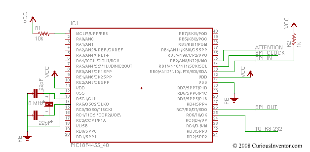
We used 2 PIC18f4550 to do the port sniffing, see below to download the code.
PIC18f4550 Code to Read a PlayStation 2 Dual Shock or Guitar Hero Controller
The first program will configure a controller in analog mode so that all the joysticks and button pressures can be read. It also sets up the Left pressure to controller the left vibration motor and the Right button pressure to toggle the smaller right vibration motor.
Each command and response packet is sent out a serial port at 57600 kbs.
The second program can operate in two modes:
- Continous SPI to Serial: Every SPI byte is sent out the serial port at 57600. Since the play station communicates at 512kbs, the code uses a circular buffer to capture SPI bytes until the playstation pauses between packets, at which time it sends out the data via serial.
- Bulk Capture and Dump: Caputer about 650 bytes of data into buffers, then dump the entire batch out through serial. We used this code to capture the initial communication between a Play Station and controller when they first connect. There are probably about 100 cleaner ways to do this, but the PICs we had on hand only had one SPI port, so two PICs were used at the same time to capture both the command and data lines. One PIC would send back it’s recordings immediately, and the other would wait for a few seconds, during which time a switch was flipped to connect the PC’s serial to the 2nd PIC.
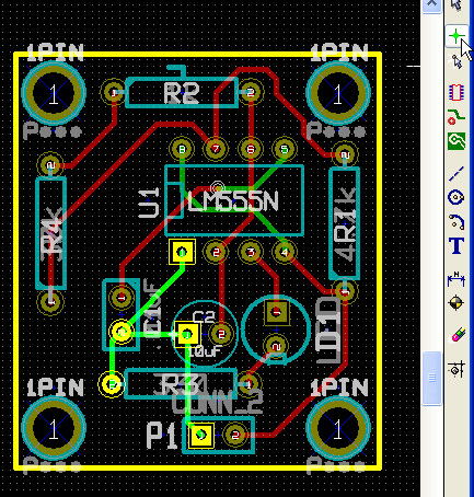
Connection Schematic:
note: avoid connecting the PIC’s SPI clock to a play station’s clock when the PIC is configured as a SPI master.