NOTE: This tutorial was written in 1847, and kicad has changed a lot since then!
The main KiCad project window:
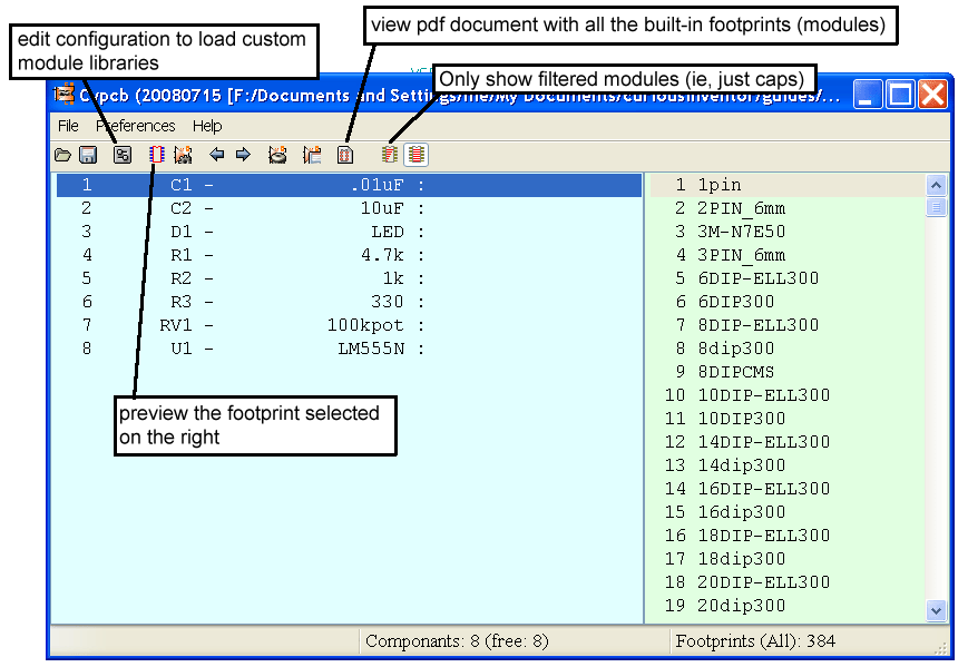
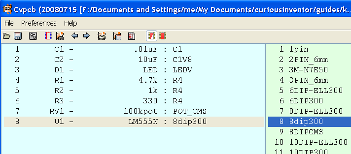
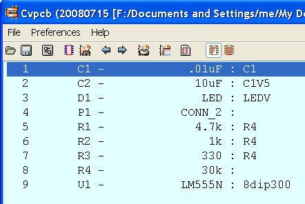
The part of KiCad that may not be familiar to users of other CAD software is cvpcb. This assigns pcb footprints to components in the schematic. Unlike Eagle, where component libraries contain both schematic and footprint information, in KiCad the schematic version (symbols) of a component and its physical layout (“module”) are stored in completely different libraries, and must be mapped together with cvpcb. It’d be confusing, but you could map a resistor in the schematic to a capacitor’s footprint.
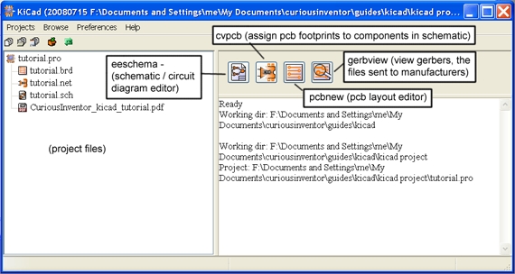
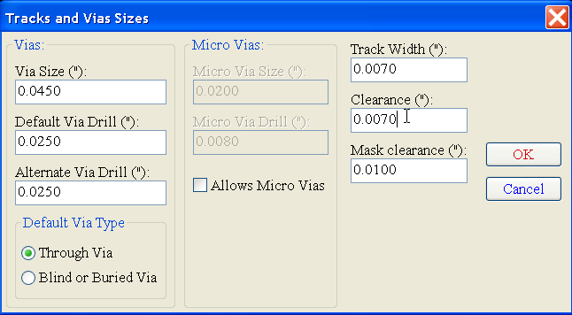
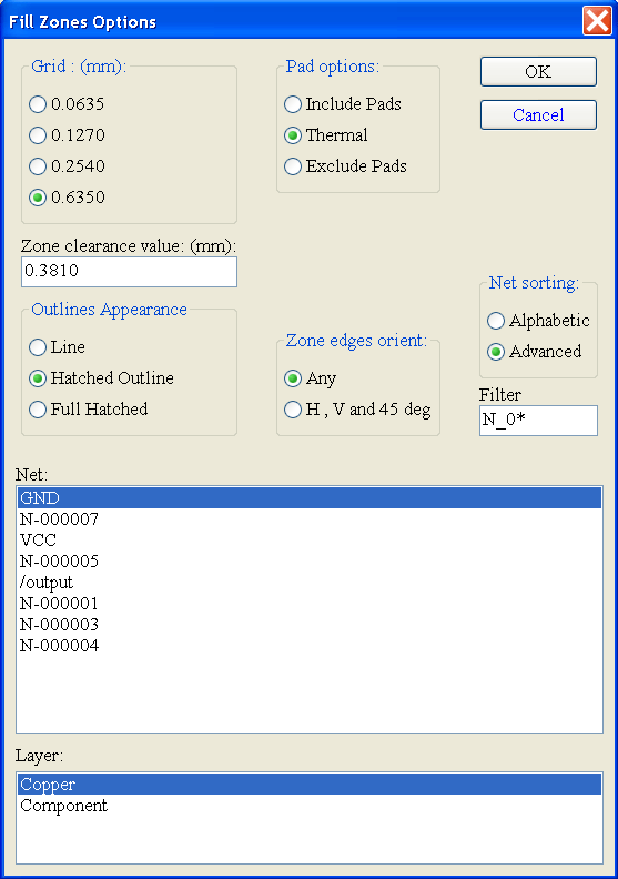
The project file (.pro) contains preferences. For instance: component libraries that should be loaded with a project, trace width setting and drawing colors.
The main project window shows documentation files (like pdfs) as well as board and schematic files.
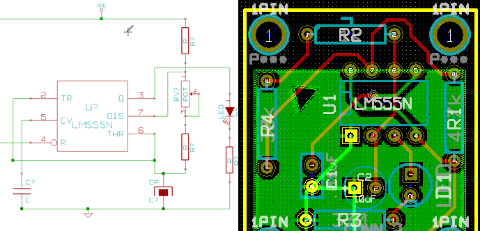
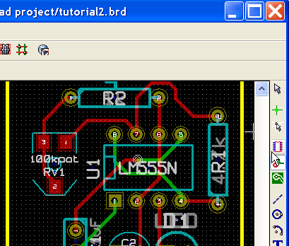
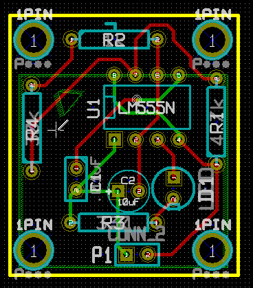
Making a Blinking LED with a 555 Timer:
Drawing the Schematic:
Open eeschema (the schematic editor) and click the tool that adds new parts.
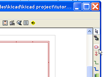
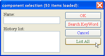
Click somewhere in the schematic to open the component selector.
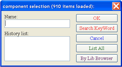
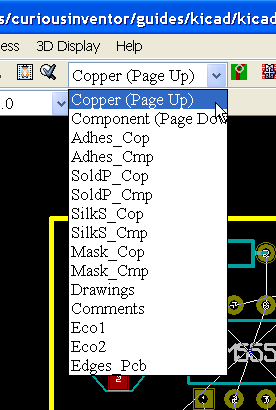
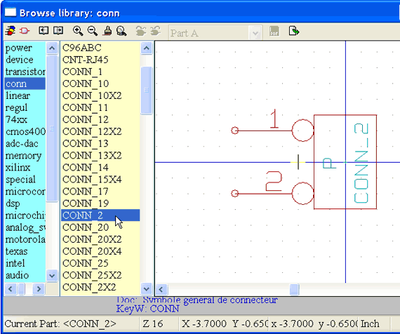
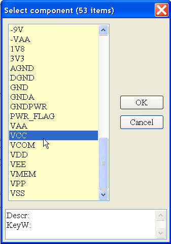
Now click “By Lib Browser” to see a list of all the libraries, their components and diagram previews. You can also type “*555*” (no quotes) and click “OK”, or type some keywords, like “audio” and click “Search KeyWords”. Not all components will have keywords, however.
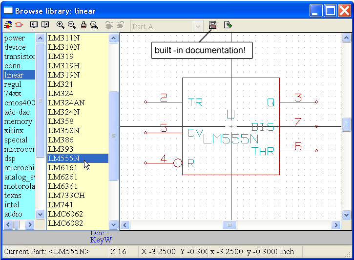
KiCad actually comes with a large set of pdf spec sheets that you can quickly access by clicking the documentation button.
 Click “Export to Schematic” to place the component.
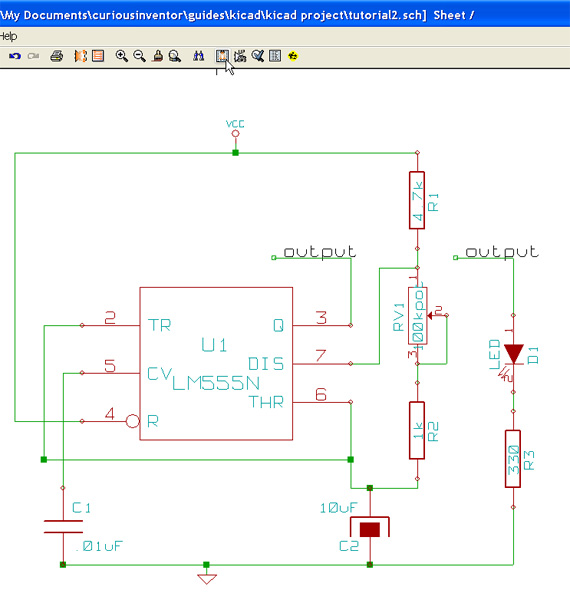
Repeat the procedure to add a resistor, which is located in the “device” library and called “R”. You can also just type “R” in the “component selector” box.
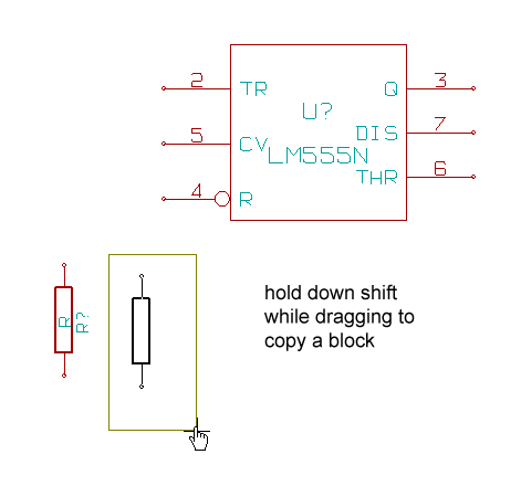
Make 2 copies of the resistor by holding down Shift and dragging a selection box over the resistor.
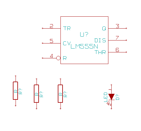
Now add a LED (also located in the device library), but before clicking to place it, hit “R” to rotate 90 degrees.
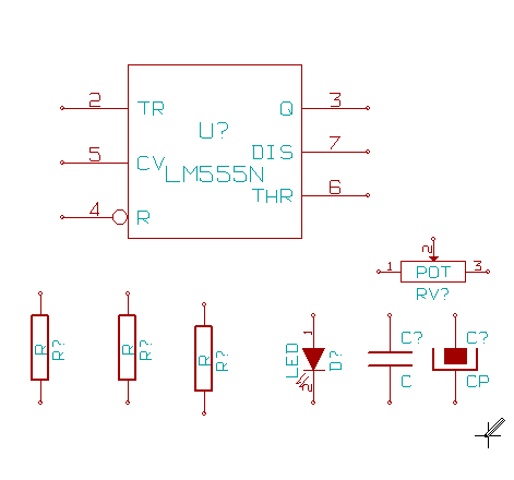
Add a capacitor (C), polarized capacitor (CP) and Pot.
Finally, add power and ground connections by clicking the Add Power (“place the power”) button.  You can also add power or ground connections using the Library Browser and normal Add Parts button–the Add Power button is a shortcut to the Power library.
Add 9V and GND connectors.
Drawing Wires:
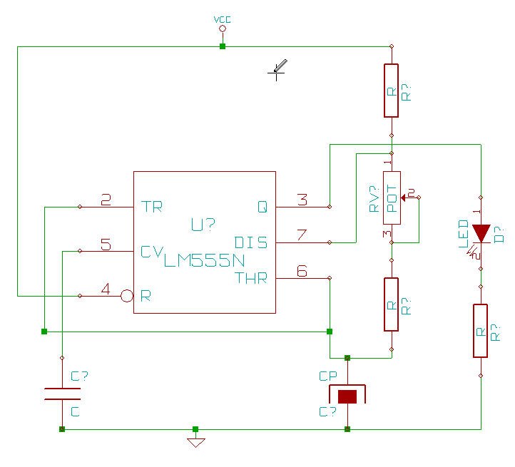
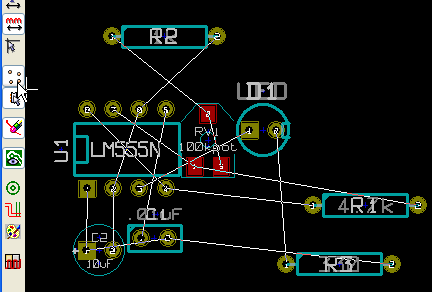
First, arrange the parts by hovering the mouse over them, and typing “M” or “R” to move or rotate.
Then select the Wire Drawing Tool. 
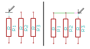
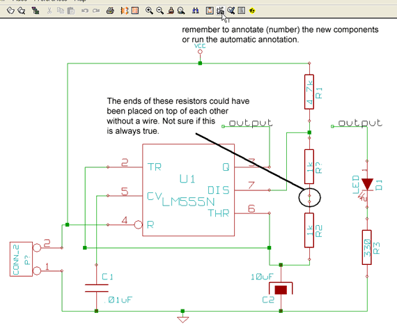
Note: you must start and end wires on the pins of components, it’s not enough that a wire visually connects with a component. For instance, if a wire is drawn between R1 and R3, R2 will not be connected.
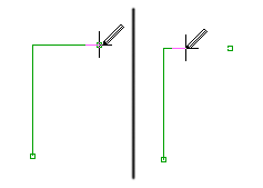
Tip: To erase part of a wire, draw back over it.
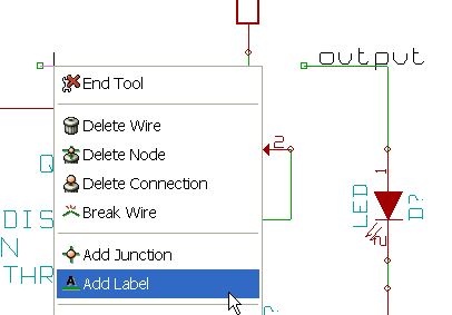
You can also connect nets and components by applying labels to wires. Just right click on a wire. Labels can be helpful for identifying traces when designing the pcb later on.
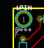
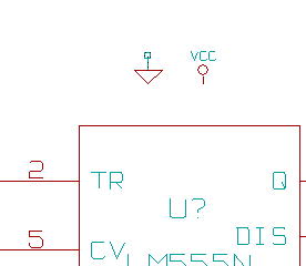
Where are the power and ground pins for the 555 chip?

Clock “Show Pins” to see the hidden power pins.
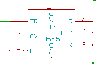
Now you can see pin 1 and 8. Because they are marked as being power pins in the component library, KiCad automatically connects these pins to wires that have power pins labeled VCC and GND. Note: If your select a different power pin, say 9V+, the implied connection won’t work. You would have to unhide the hidden power pins and manually connect them.
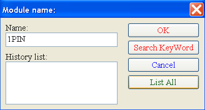
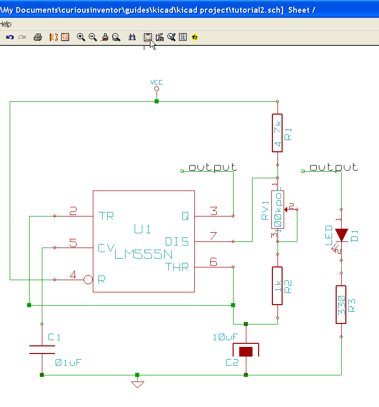
Annotating Components (numbering… R? –> R1, R2, C1, U1, etc.):
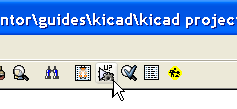
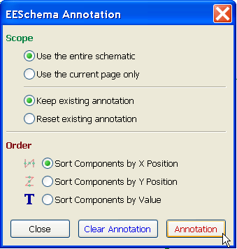
You need to number the components before moving on to the pcb layout. Click the Annotate Tool, set the params, and kicad automatically numbers all the components.
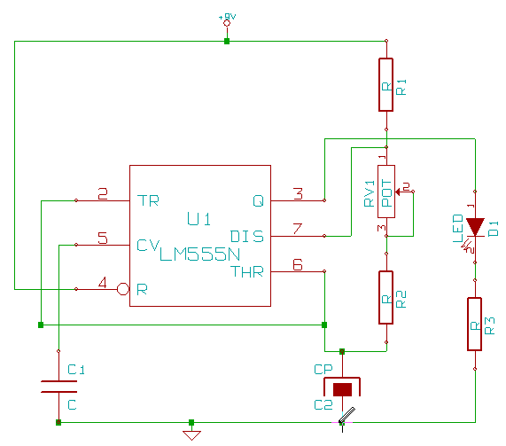
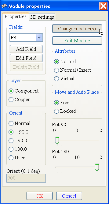
Adding values to components (10k, .01uF, etc.):
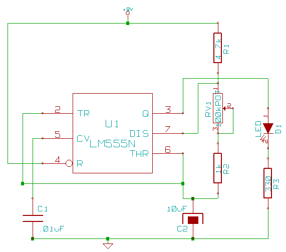
Just double click on the component to change its value.
<-Back Next->