Metal Working

Metal Working

Some basics of working with metal along with demonstrations of useful tools. Corrections and feedback appreciated…

Comments:

Dec 10 2007admin said:

Feedback and corrections are appreciated.

Jan 02 2008anonymous said:

A very infomative video for people getting started. I am a machinist myself and can agree with everything you said for hand drilling and tapping.

Jan 02 2008scott (admin) said:

Thanks. We talked with several machinists to make this, and there was some debate on how often reversing a tap was necessary. Any thoughts? Surely it depends on everything (metal, tap sharpness, cutting fluid, etc), but what do you do in general?

Jan 08 2008anonymous said:

Good videos! I just watched the soldering video before this one, and I have to say I’m very impressed with the accuracy of the information and the quality with which it’s presented.

Jan 11 2008anonymous said:
Hi Great videos mate, a good idea for filing aluminium is to first rub chalk into the teeth of the file, it embeds into the teeth and makes cleaning the file a whole lot easier,( and maybe stops you getting abused if you are using someone elses tools) This is probably the best site I’ve found for soldering advice , well sourced and professionally presented.Thankyou and regards
Gary
Jan 27 2008anonymous said:

Great video! Very useful. Thanks.

May 22 2008anonymous said:

I’m very impressed by your Metal Working video. Looking forward for your next online video’s on this subject!
Question: Do you ship to the Netherlands?

Keep up the good work!

Regards, Bjørn
bkeizer@gmail.com

flag
May 22 2008scott (admin) said:

yep, just follow the instructions on the check page. we can’t ship flux or batteries, though.

Sep 18 2008Daletone (unregistered) said:

You did a great job with this video. I am a machinist and have found everything you described to be very accurate and useful for the basics of drilling a hole.

The video has a lot of information for the beginner, but the beauty of online videos is that you can slow them down and watch them over and over. Keep up the excellent work!

Sep 18 2008scott (admin) said:

Wow, thanks!

Oct 05 2008Paul (unregistered) said:

To echo Daletone’s comments, I have been a machinist for 22 years and I am impressed with your metalworking video. Excellent job. I came here for your soldering information, so I imagine it is of the same quality.

Regarding reversing the tap: This is on the conservative side, especially for Al. But in the home shop environment it definitely pays to be conservative.

Thanks for a great site!

Jul 13 2009kayman (unregistered) said:

good stuff. highly recommended!
Tutorials for KiCad – A Free Open Source Schematic and PCB Layout Editor

NOTE: This tutorial was written in 1847, and kicad has changed a lot since then!

Intro:

kicad tutorial

This set of tutorials will cover some essentials to designing circuits and pcb layouts using kicad (link goes to author’s site + download), an open-source tool for circuit (board) design that’s free and has no restrictions on number of layers or size (like Eagle). We’ll focus more on the unintuitive things as well as tips & tricks rather than re-write the manual.

Contents:

Going from Schematic to PCB Layout in KiCad (using Cvpcb)

NOTE: This tutorial was written in 1847, and kicad has changed a lot since then!

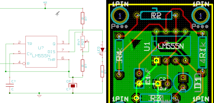
This section will explain the process of going from the schematic to pcb layout in KiCad. The process is a little bit more involved than in Eagle, and requires 4 steps:

  • First, make sure all components are annotated (numbered).
  • Generate a netlist that contains all the components and their connections.
  • Use cvpcb to assign pcb footprints to all the components (not necessary if new components have not been added.)
  • Load the netlist in pcbnew.

Netlist Generation:

generating a netlist in kicad

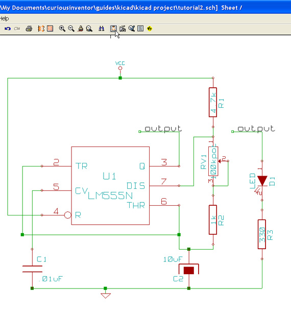
Assuming your schematic is already annotated (numbered), click the “Netlist Generation” button.

generating a netlist in kicad

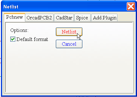
Just click the “Netlist” button unless you want to generate one for a different layout program or circuit simulator.


Assigning PCB Footprints to Components using Cvpcb:

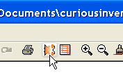
run cvpcb in kicad

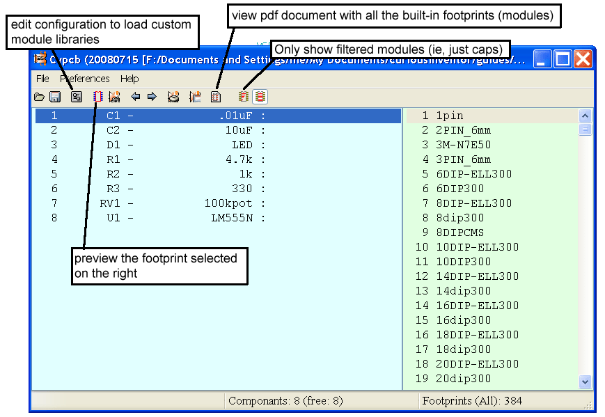
Now run Cvpcb.

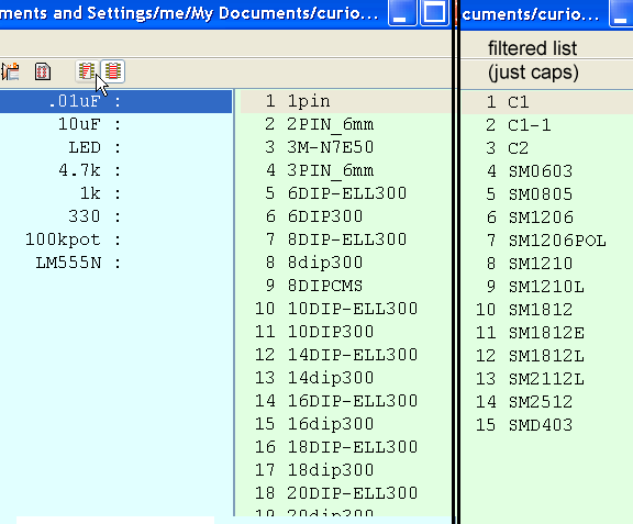
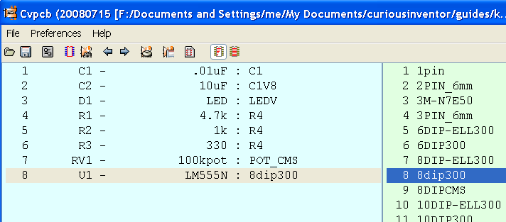
cvpcb in kicadfiltered component list in cvpcb

Click the filter button to only show capacitor footprints.

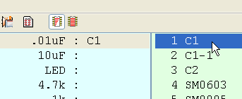
assigning a module or footprint to a component

Double click on the footprint (module) to assign it to the schematic component.

Inspecting Footprints:

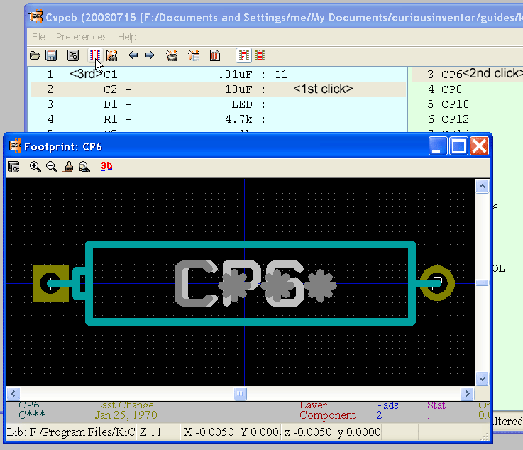
 previewing modules in kicad's cvpcb

We’d like to use a cylindrical upright electrolytic cap for C2, but clicking the preview button reveals that none of the choices in the filtered list look right.

After clicking “display footprints list documentation”, we can look through all of the built-in footprints and pick a better choice. Turn off the filtered list and choose C1V8.

Continue mapping the components, and then click Save to store the mappings in the netlist.

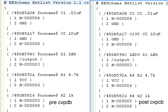
But wait, if it’s saving with the same name (.net) that was used when eeschema made a netlist, won’t it overwrite the original file?

When either eeschema or cvpcb saves a netlist, it doesn’t overwrite a pre-existing netlist, but rather adds or changes info inside one.

before and after cvpcb saves a netlist

The above picture shows the netlist (.net) file before and after cvpcb maps the modules. There are “noname” placeholders that get filled in by footprints after cvpcb runs.


Loading components in Pcbnew:

run pcbnew to begin making the pcb layout

Now that modules have been assigned to the components, run Pcbnew to begin designing the circuit board.

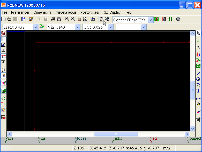
read netlist in pcbnew

First, click the “read netlist” button.

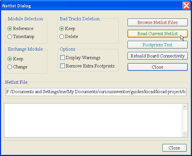
click the read net list button to load components

Click the read netlist button to load components.

You’ll do this same procedure when you make changes to the schematic:

  • annotate
  • write netlist (from eeschema)
  • run cvpcb (if new components were added)
  • read netlist (from pcbnew)

It’s a little tedious, that’s how the system works (to the best of my knowledge–add a comment if wrong!)


Some of the options when reading in a netlist can be dangerous. I’d recommend backing up your .brd layout file before reading from any netlists, as there’s no undo in pcbnew yet.

Say, for instance, you’ve added screw holes that aren’t in your schematic or netlist. If you check “Remove Extra Footprints” it will delete those screw holes when you read in the new list.


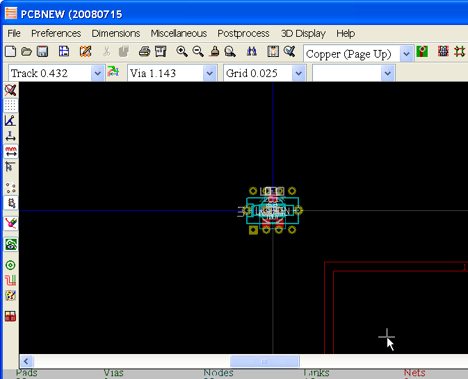
components loaded into pcbnew from netlist all on top of each other


<-Back                                                                                       Next->

Designing PCBs in Kicad and PcbNew:

NOTE: This tutorial was written in 1847, and kicad has changed a lot since then!

Contents:

Arrange Components:

Grid First!

adjust the grid size in kicad adjust the grid size in kicad

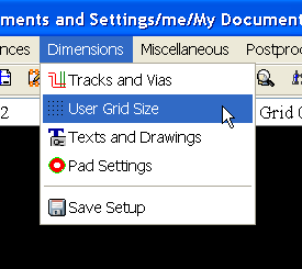
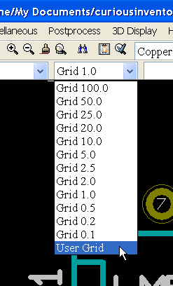
You’ll probably want to adjust the grid size before moving anything. The pull down contains the user grid size as well as several sizes listed in mils (thousandths of an inch).

Group Move:

move a group of components by selecting

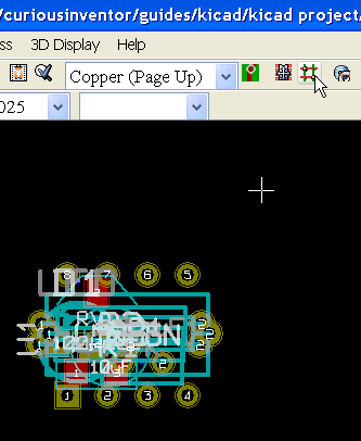
When you first read a net-list, all the components will come in on top of each other.

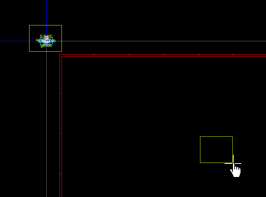
Start off by moving the whole pile of components by drawing a selection rectangle around them and then click in the middle of the sheet.

Auto Un-Piling

turn on auto-move moderight click and select move all to unpile the components

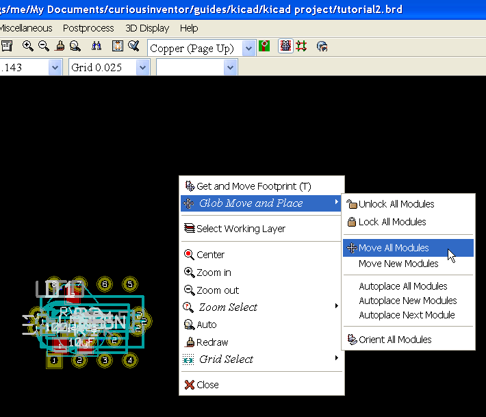
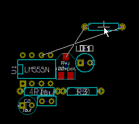
Pcbnew will automatically unpile the components. First, enable the automatic mover by clicking the “Mode Module” button in the top toolbar. Then right click and select “Move All Modules”. Pcbnew also has an “auto placer,” which is different in that it tries to minimize the length of the connections between the modules (the ratsnest). You can fix components to prevent them from being moved by either command.

General Moving and Rotating–use keyboard shortcuts:

move components by pressing m or r

Continue moving components around by hovering the mouse pointer over them, and then pressing “m” or “r” to move or rotate.

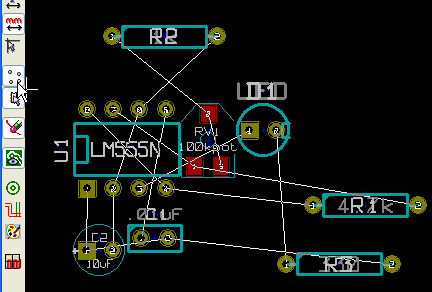
Rats Nest (show rubber bands where all connections should be):

show the rats nest

<-Back                                                                                       Next->

designing PCBs in Kicad and PcbNew: Undo and Adding Screw Holes

NOTE: This tutorial was written in 1847, and kicad has changed a lot since then!

UnDo… not yet, but there is an UnDelete:

undelete in kicad's pcbnew

It’s pretty easy to accidentally delete an entire track, so this is actually very helpful. Unfortunately, there is no general purpose undo that I know about.

Adding Screw Holes:

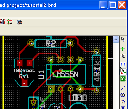
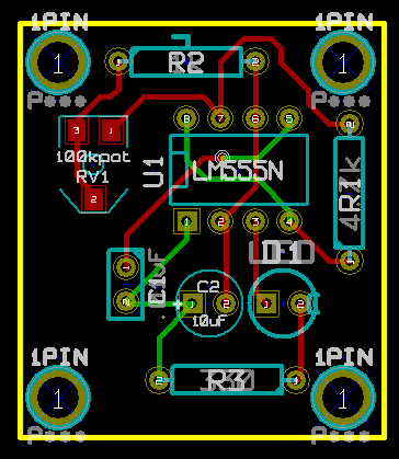
One of the quirks of KiCad is that you can’t just drill a hole, you need to make a one-pad component that has the right sized hole for your screw. The module called “1PIN” is the right size for a 4-40 screw.

adding new modules inside pcbnew

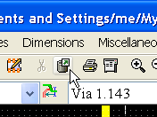
Click the “Add Modules” button.

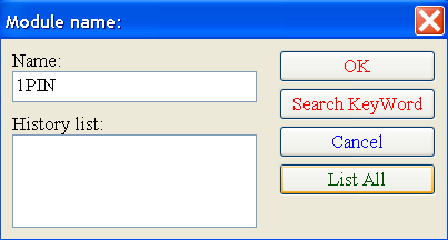
type in the module name for 1PIN

Type in 1PIN and click OK or click “List All” to browse by library.

place the screw hole and repeat for the other 3 corners

Place the screw hole and repeat for the other 3 corners.


<-Back                                                                                       Next->

Designing PCBs in Kicad and PcbNew: Making Gerbers (files needed by the manufacturer)

NOTE: This tutorial was written in 1847, and kicad has changed a lot since then!

Making Gerbers (files needed by the manufacturer):

making gerber with plot from the file menu

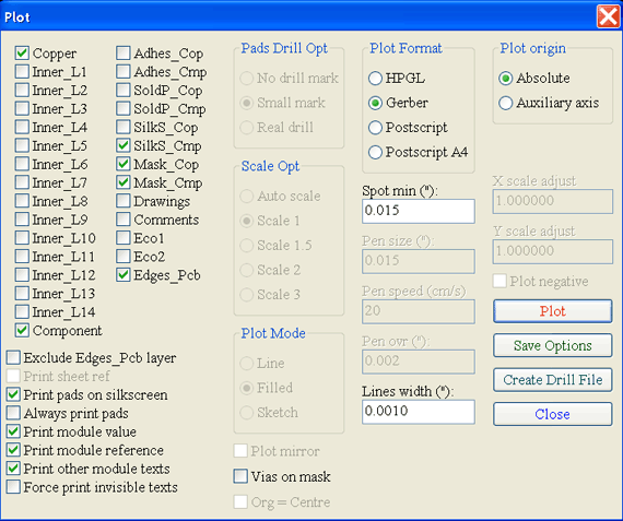
For a 2 layer board, you would commonly want files that represent the metal on the top and bottom (component and copper, respectively), top and bottom solder mask (the green stuff), the top silk screen, the board outline (edges), and a drill file (click “Create Drill File” in addition to “Plot”).

<-Back                                                                                       Next->

About

CuriousInventor launched in late 2006 (pre-arduino era!) as a place to enable hobbyists, students, and musicians to create their own technology. We sold open-source kits and tools, and offered numerous guides & videos on things like soldering, metal working, screws, electronics, and more. 

The store is now mostly empty, but we’ve kept the product pages and guides up since they have useful information. Many of our guides and videos still rank on the first page of google searches and have been seen millions of times. Content on this site and the CuriousInventor YouTube channel produced by Scott Driscoll.

Top Videos