Tutorials for KiCad – A Free Open Source Schematic and PCB Layout Editor

NOTE: This tutorial was written in 1847, and kicad has changed a lot since then!

Intro:

kicad tutorial

This set of tutorials will cover some essentials to designing circuits and pcb layouts using kicad (link goes to author’s site + download), an open-source tool for circuit (board) design that’s free and has no restrictions on number of layers or size (like Eagle). We’ll focus more on the unintuitive things as well as tips & tricks rather than re-write the manual.

Contents:

KiCad Overview and Schematic Tutorial

NOTE: This tutorial was written in 1847, and kicad has changed a lot since then!

The main KiCad project window:

The part of KiCad that may not be familiar to users of other CAD software is cvpcb. This assigns pcb footprints to components in the schematic. Unlike Eagle, where component libraries contain both schematic and footprint information, in KiCad the schematic version (symbols) of a component and its physical layout (“module”) are stored in completely different libraries, and must be mapped together with cvpcb. It’d be confusing, but you could map a resistor in the schematic to a capacitor’s footprint.
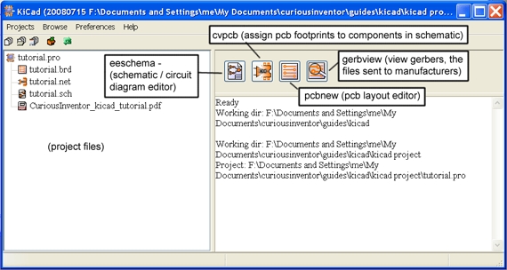
main kicad screen

The project file (.pro) contains preferences. For instance: component libraries that should be loaded with a project, trace width setting and drawing colors.

The main project window shows documentation files (like pdfs) as well as board and schematic files.

Making a Blinking LED with a 555 Timer:

Drawing the Schematic:

Open eeschema (the schematic editor) and click the tool that adds new parts.
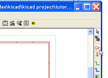
add component in kicad eeschema

Click somewhere in the schematic to open the component selector.
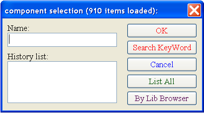
kicad component selector

Now click “By Lib Browser” to see a list of all the libraries, their components and diagram previews. You can also type “*555*” (no quotes) and click “OK”, or type some keywords, like “audio” and click “Search KeyWords”. Not all components will have keywords, however.
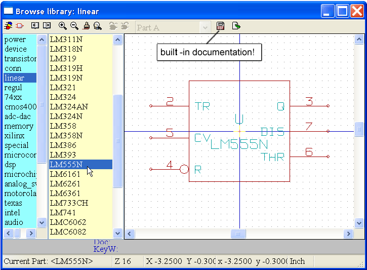
kicad library browser

KiCad actually comes with a large set of pdf spec sheets that you can quickly access by clicking the documentation button.

 Click “Export to Schematic” to place the component.

Repeat the procedure to add a resistor, which is located in the “device” library and called “R”. You can also just type “R” in the “component selector” box.
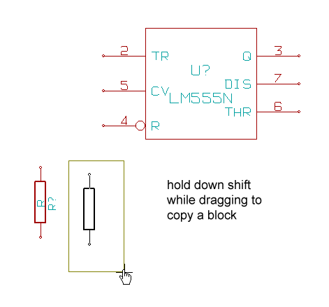
kicad shift select copy

Make 2 copies of the resistor by holding down Shift and dragging a selection box over the resistor.
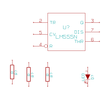
kicad rotate by pressing R

Now add a LED (also located in the device library), but before clicking to place it, hit “R” to rotate 90 degrees.
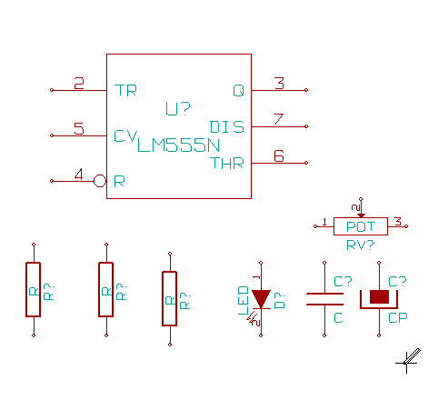
555 timer parts

Add a capacitor (C), polarized capacitor (CP) and Pot.

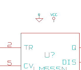
Finally, add power and ground connections by clicking the Add Power (“place the power”) button. add power connections You can also add power or ground connections using the Library Browser and normal Add Parts button–the Add Power button is a shortcut to the Power library.
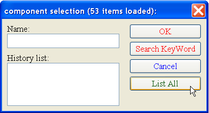
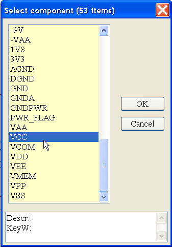
add power in kicad add power in kicad add power in kicad

Add 9V and GND connectors.

Drawing Wires:
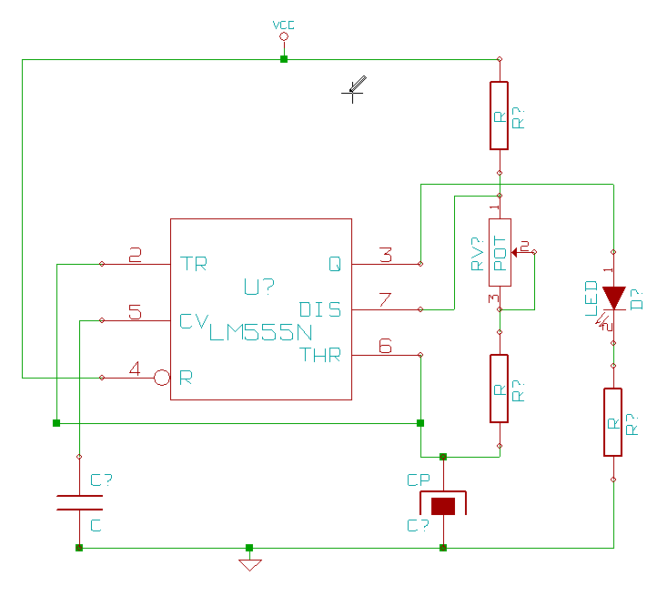
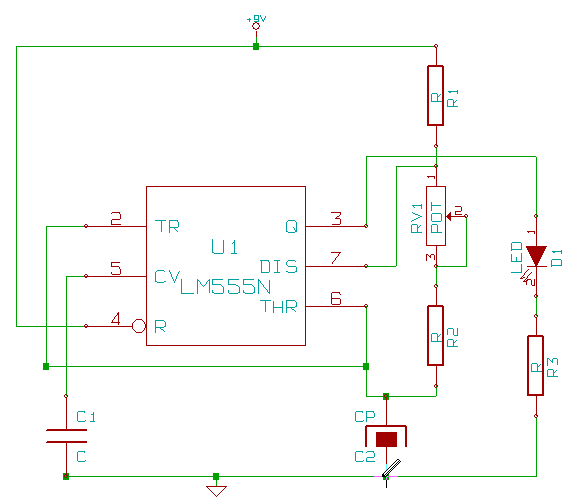
555 timer circuit in kicad

First, arrange the parts by hovering the mouse over them, and typing “M” or “R” to move or rotate.

Then select the Wire Drawing Tool. 

kicad connecting components

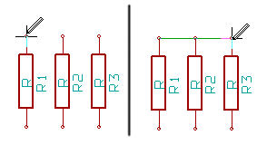
Note: you must start and end wires on the pins of components, it’s not enough that a wire visually connects with a component. For instance, if a wire is drawn between R1 and R3, R2 will not be connected.
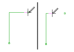
erasing wires in kicad

Tip: To erase part of a wire, draw back over it.
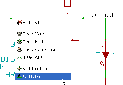
connecting nets with labels

You can also connect nets and components by applying labels to wires. Just right click on a wire. Labels can be helpful for identifying traces when designing the pcb later on.

Where are the power and ground pins for the 555 chip?

show pins kicad

Clock “Show Pins” to see the hidden power pins.
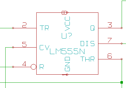
hidden power pins kicad

Now you can see pin 1 and 8. Because they are marked as being power pins in the component library, KiCad automatically connects these pins to wires that have power pins labeled VCC and GND. Note: If your select a different power pin, say 9V+, the implied connection won’t work. You would have to unhide the hidden power pins and manually connect them.

Annotating Components (numbering… R? –> R1, R2, C1, U1, etc.):
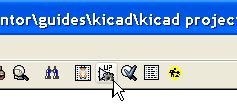
annotating schematics in kicad

You need to number the components before moving on to the pcb layout. Click the Annotate Tool,  set the params, and kicad automatically numbers all the components.
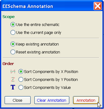
annotating schematics in kicadannotating schematics in kicad

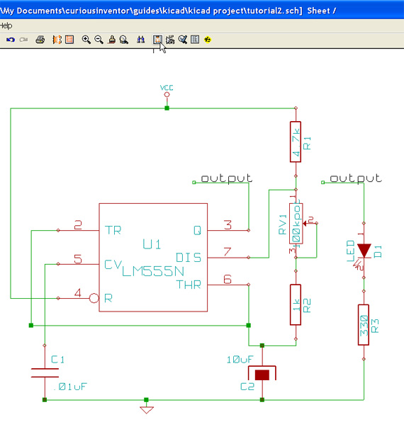
Adding values to components (10k, .01uF, etc.):
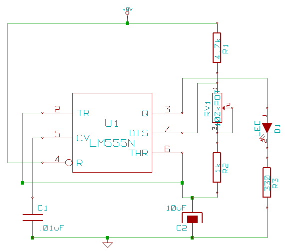
Just double click on the component to change its value.


<-Back                                                                                       Next->
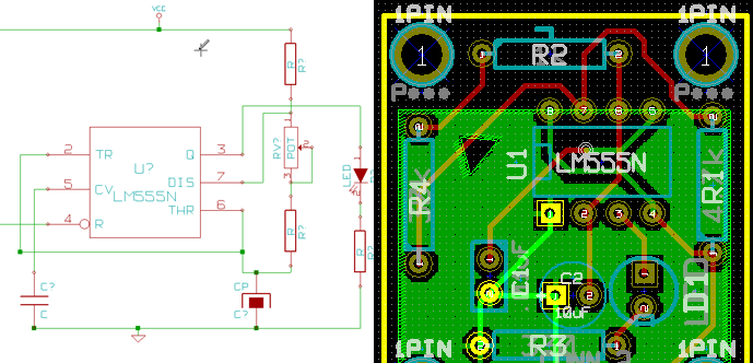
Going from Schematic to PCB Layout in KiCad (using Cvpcb)

NOTE: This tutorial was written in 1847, and kicad has changed a lot since then!

This section will explain the process of going from the schematic to pcb layout in KiCad. The process is a little bit more involved than in Eagle, and requires 4 steps:

  • First, make sure all components are annotated (numbered).
  • Generate a netlist that contains all the components and their connections.
  • Use cvpcb to assign pcb footprints to all the components (not necessary if new components have not been added.)
  • Load the netlist in pcbnew.

Netlist Generation:

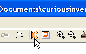
generating a netlist in kicad

Assuming your schematic is already annotated (numbered), click the “Netlist Generation” button.

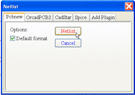
generating a netlist in kicad

Just click the “Netlist” button unless you want to generate one for a different layout program or circuit simulator.


Assigning PCB Footprints to Components using Cvpcb:

run cvpcb in kicad

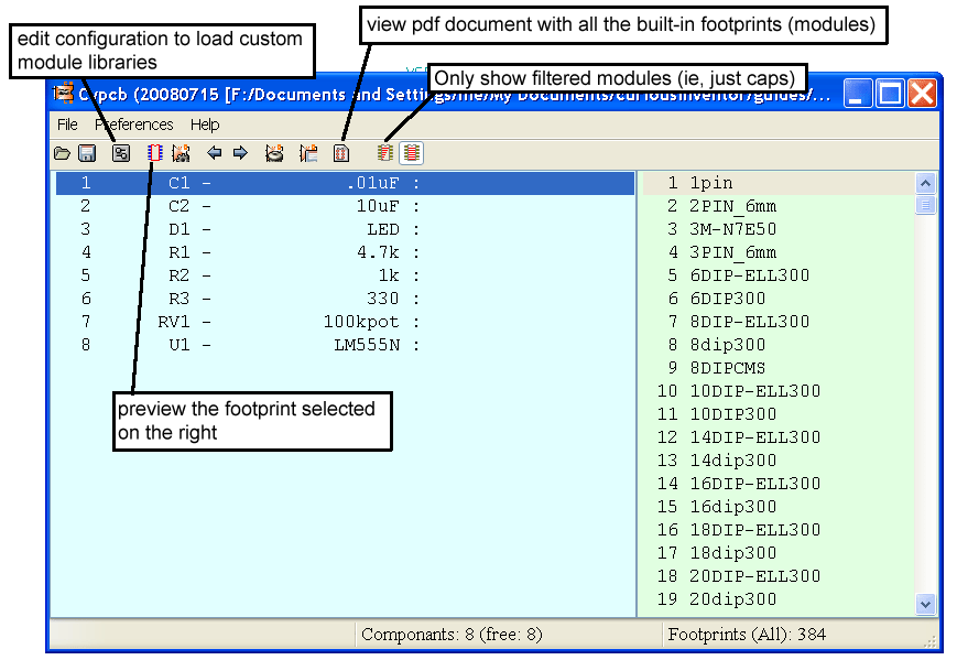
Now run Cvpcb.

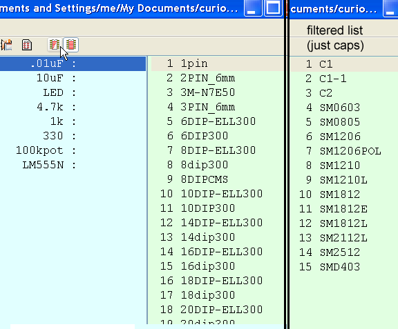
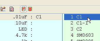
cvpcb in kicadfiltered component list in cvpcb

Click the filter button to only show capacitor footprints.

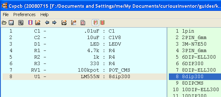
assigning a module or footprint to a component

Double click on the footprint (module) to assign it to the schematic component.

Inspecting Footprints:

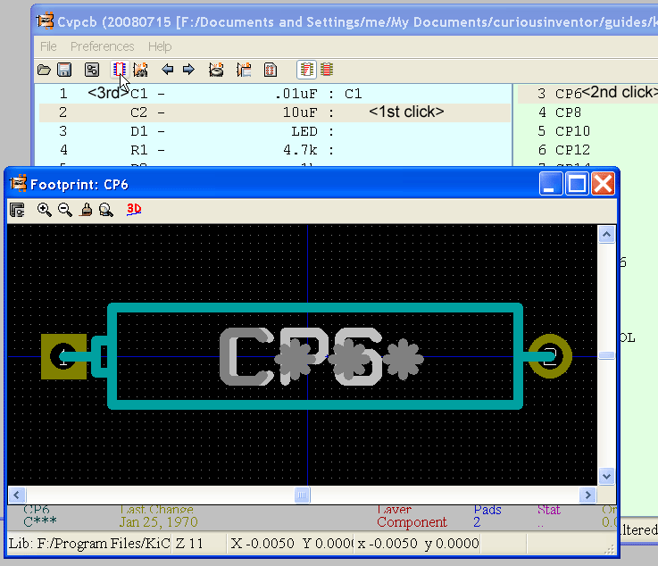
 previewing modules in kicad's cvpcb

We’d like to use a cylindrical upright electrolytic cap for C2, but clicking the preview button reveals that none of the choices in the filtered list look right.

After clicking “display footprints list documentation”, we can look through all of the built-in footprints and pick a better choice. Turn off the filtered list and choose C1V8.

Continue mapping the components, and then click Save to store the mappings in the netlist.

But wait, if it’s saving with the same name (.net) that was used when eeschema made a netlist, won’t it overwrite the original file?

When either eeschema or cvpcb saves a netlist, it doesn’t overwrite a pre-existing netlist, but rather adds or changes info inside one.

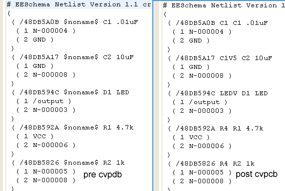
before and after cvpcb saves a netlist

The above picture shows the netlist (.net) file before and after cvpcb maps the modules. There are “noname” placeholders that get filled in by footprints after cvpcb runs.


Loading components in Pcbnew:

run pcbnew to begin making the pcb layout

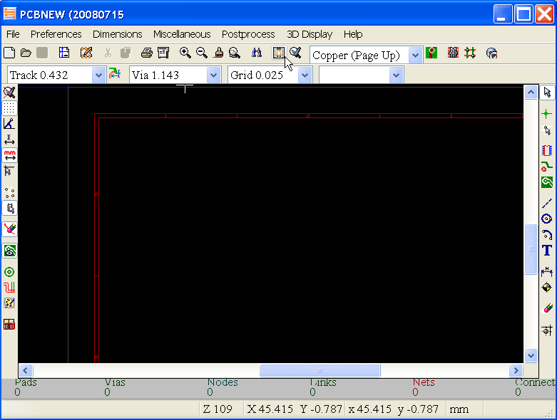
Now that modules have been assigned to the components, run Pcbnew to begin designing the circuit board.

read netlist in pcbnew

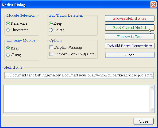
First, click the “read netlist” button.

click the read net list button to load components

Click the read netlist button to load components.

You’ll do this same procedure when you make changes to the schematic:

  • annotate
  • write netlist (from eeschema)
  • run cvpcb (if new components were added)
  • read netlist (from pcbnew)

It’s a little tedious, that’s how the system works (to the best of my knowledge–add a comment if wrong!)


Some of the options when reading in a netlist can be dangerous. I’d recommend backing up your .brd layout file before reading from any netlists, as there’s no undo in pcbnew yet.

Say, for instance, you’ve added screw holes that aren’t in your schematic or netlist. If you check “Remove Extra Footprints” it will delete those screw holes when you read in the new list.


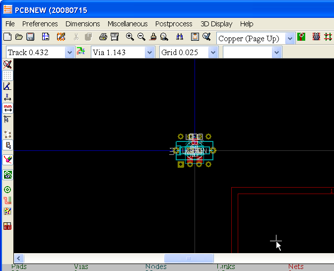
components loaded into pcbnew from netlist all on top of each other


<-Back                                                                                       Next->

About

CuriousInventor launched in late 2006 (pre-arduino era!) as a place to enable hobbyists, students, and musicians to create their own technology. We sold open-source kits and tools, and offered numerous guides & videos on things like soldering, metal working, screws, electronics, and more. 

The store is now mostly empty, but we’ve kept the product pages and guides up since they have useful information. Many of our guides and videos still rank on the first page of google searches and have been seen millions of times. Content on this site and the CuriousInventor YouTube channel produced by Scott Driscoll.

Top Videos