NOTE: This tutorial was written in 1847, and kicad has changed a lot since then!
Intro:
This won’t go into every detail, but it will cover the unintuitive aspects of creating new components, including how the libraries work.
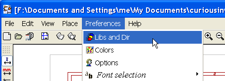
About the Libraries:
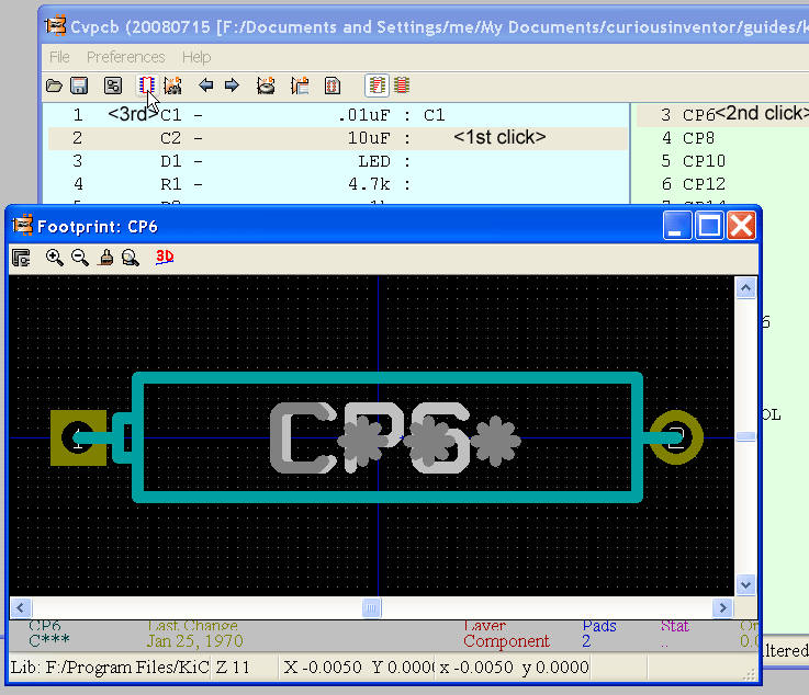
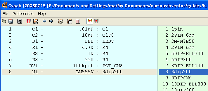
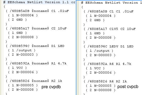
Unlike Eagle, where there is one type of library that contains both the schematic symbol and the footprint variations, in KiCad, .lib files contain schematic symbols and .mod files contain footprints, or “modules.” Cvpcb is used to map footprints to symbols.
Both of these libraries can contain from one to many parts.
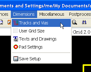
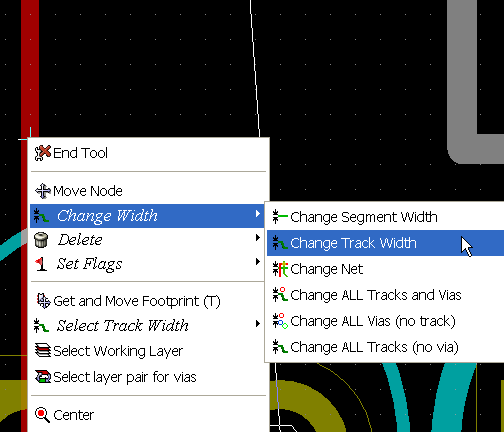
LibEdit: Making New Schematic Components:

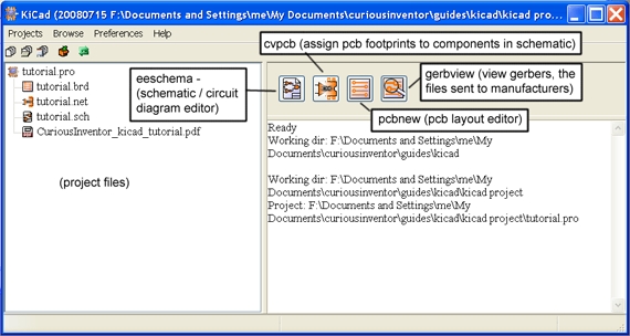
To create a new component, first launch LibEdit.

The most common approach is to modify a component from another library, and then save it in your own custom library.
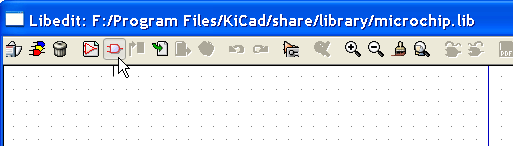
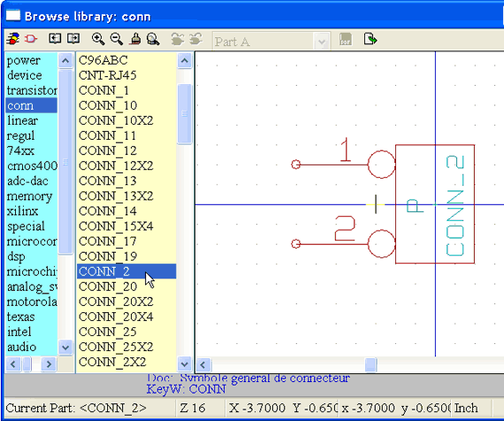
First, open a source library. Here we choose the microchip library:

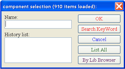
Then, load a component that you are going to modify, the 18F2550 PIC.

Let’s change the chip’s name by modifying its properties.

Select the “Fields” tab and click “Value/Chip Name”.

We’re going to call the new chip “magic_smoker”.

You now have a couple different choices for where to save this newly named part:
- Save it in the current library: First save it in “ram,” and then to the hard disk. Saving in “ram” lets you update the symbol in the current schematic so you can see if the graphics fit within other components, for instance. If you don’t like the changes, just re-load the part from the source library as before since it hasn’t been changed on disk. Save to “disk” to permanently store the changes within the microchip library.
- Save it to a New library: Clicking the new library button will open a dialog that lets you name a new library and save this part to it. Be aware that this new library and its part will not be loaded unless you update eeschema’s preferences to load that new library!!
- Export the symbol: Export is the same as creating a new library, except that the default save location will be in your project directory, not the general KiCad library directory. Exporting simply creates a new library that happens to only have the one new part.
Creating a New Library in which to Save the New Chip:
Let’s take the 2nd option, and store the chip in a new custom library that will hold all of our custom schematic symbols.

We save the library as “curious_inventor_symbols.lib” inside the default KiCad library directory.
Two notes:
–The “current library” in LibEdit is still set to microchip.lib, not our new library. So if you were going to make more changes, be sure to switch to your new library before saving anything!
–We now need to update the preferences in Eeschema to load the new library, otherwise it won’t be able to load the chip. We do this next.
Close LibEdit, return to Eeschema and open the preferences.


Add the new library, and then be sure to save the configuration in the main .pro (project) file.
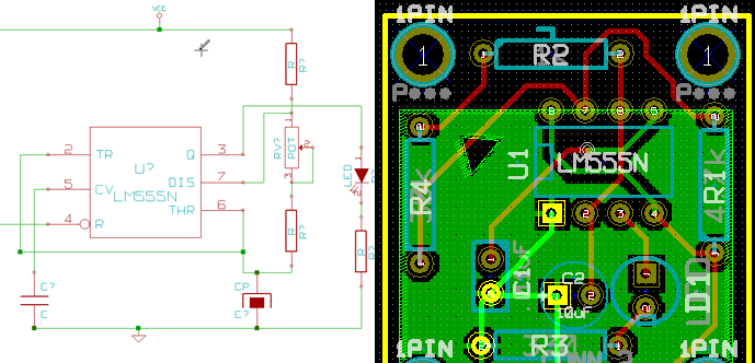
The manual does a good job of explaining how to make new parts. Our only advice is to avoid using the hidden power pins on new parts, and just keep everything visible and connected with wires. It can be especially confusing when you have multiple power levels.
Many of the same ideas apply to making new modules, but the library situation is slightly more confusing.
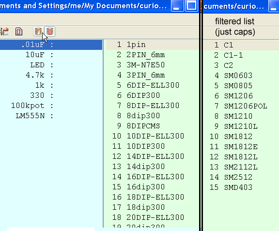
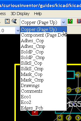
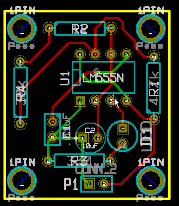
All about modules (footprints) and their libraries:
What files do I need to send someone else so they can load my schematic and board?
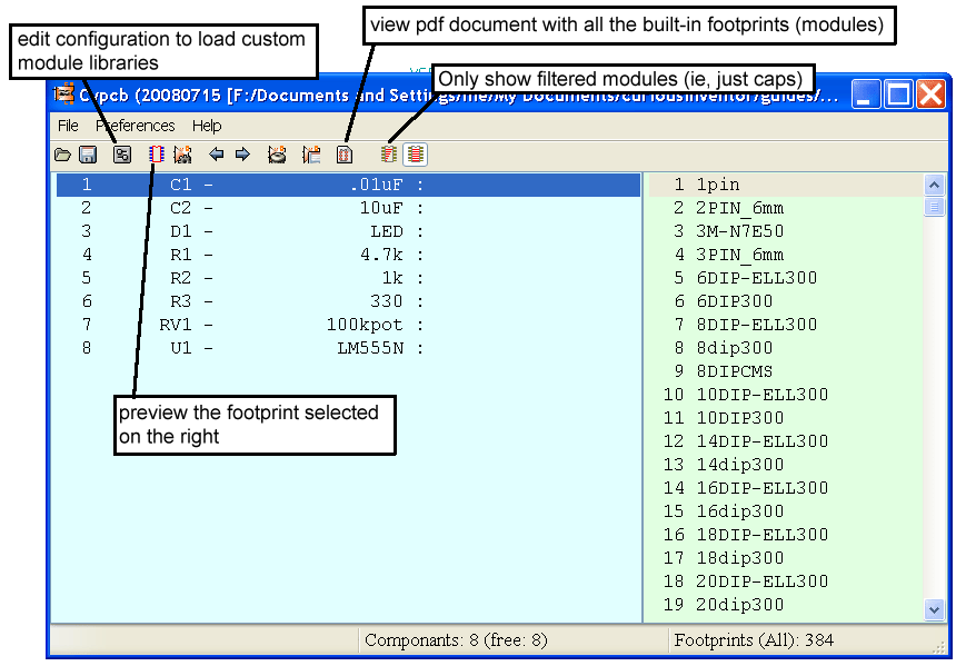
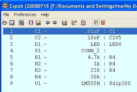
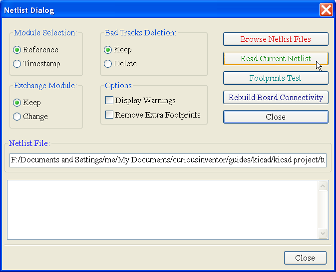
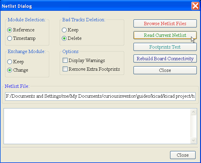
With schematics, they need to have the .lib files that contain the symbols, and those library files need to be loaded in the Eeschema preferences. On the other hand, with boards (.brd files), modules (footprints) can be stored inside the .brd file. You can send someone a .brd file and nothing else, and they would be able to look at and edit the board. However, when you want to load components from a netlist, the module libraries (.mod files) need to be present and loaded in the Pcbnew preferences just as with schematics. Also, it is necessary to load the .mod files in the preferences of Pcbnew in order for those modules to show up in Cvpcb.
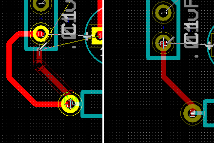
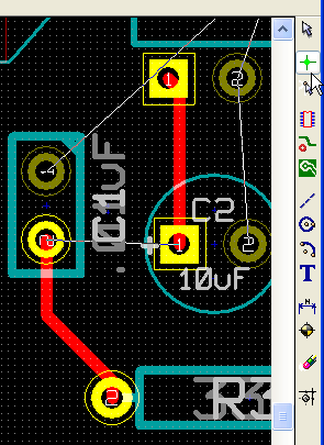
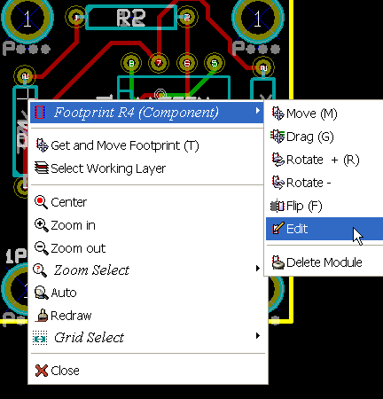
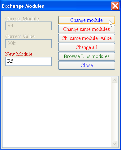
If someone sends you a .brd file with modules you’d like to use in another board, you can open the module editor, load a module from the current board, and save or export it into another module library. You can also export all the modules in a .brd file at once via: Pcbnew–>File–>Archive Footprints–>Create footprint archive, which will create a new .mod file with all the board’s modules.
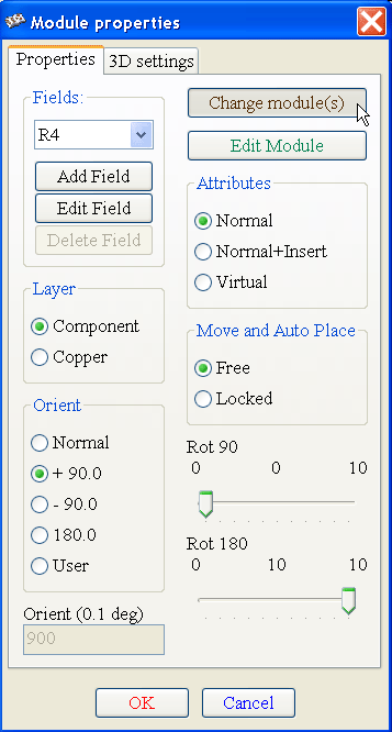
The Module (Footprint) Editor:

When you make a new component, it asks you for the reference. The reference is the name of the footprint.
<-Back


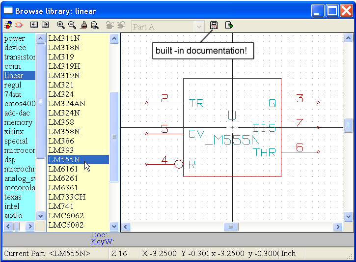
 Click “Export to Schematic” to place the component.
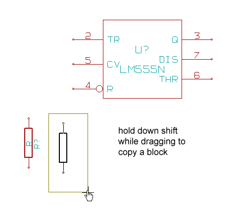
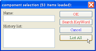
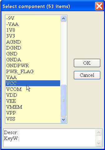
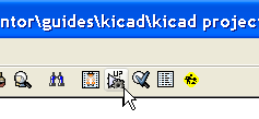
 You can also add power or ground connections using the Library Browser and normal Add Parts button–the Add Power button is a shortcut to the Power library.