NOTE: This tutorial was written in 1847, and kicad has changed a lot since then!
The main KiCad project window:
The part of KiCad that may not be familiar to users of other CAD software is cvpcb. This assigns pcb footprints to components in the schematic. Unlike Eagle, where component libraries contain both schematic and footprint information, in KiCad the schematic version (symbols) of a component and its physical layout (“module”) are stored in completely different libraries, and must be mapped together with cvpcb. It’d be confusing, but you could map a resistor in the schematic to a capacitor’s footprint.
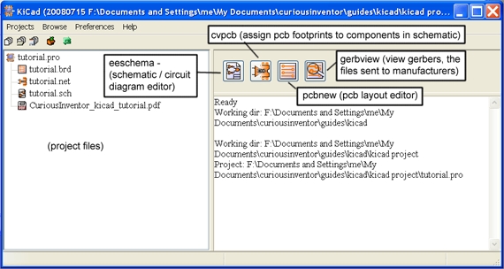
The project file (.pro) contains preferences. For instance: component libraries that should be loaded with a project, trace width setting and drawing colors.
The main project window shows documentation files (like pdfs) as well as board and schematic files.
Making a Blinking LED with a 555 Timer:
Drawing the Schematic:
Open eeschema (the schematic editor) and click the tool that adds new parts.
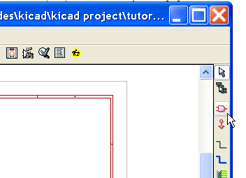
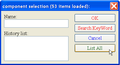
Click somewhere in the schematic to open the component selector.

Now click “By Lib Browser” to see a list of all the libraries, their components and diagram previews. You can also type “*555*” (no quotes) and click “OK”, or type some keywords, like “audio” and click “Search KeyWords”. Not all components will have keywords, however.
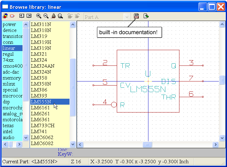
KiCad actually comes with a large set of pdf spec sheets that you can quickly access by clicking the documentation button.
 Click “Export to Schematic” to place the component.
Repeat the procedure to add a resistor, which is located in the “device” library and called “R”. You can also just type “R” in the “component selector” box.
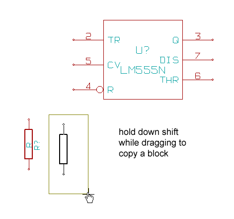
Make 2 copies of the resistor by holding down Shift and dragging a selection box over the resistor.
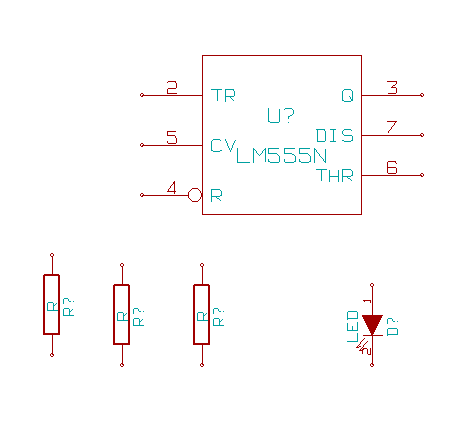
Now add a LED (also located in the device library), but before clicking to place it, hit “R” to rotate 90 degrees.
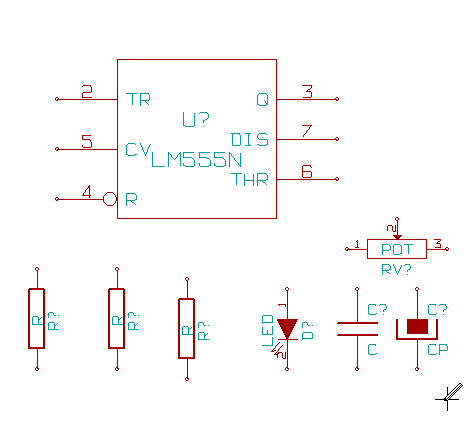
Add a capacitor (C), polarized capacitor (CP) and Pot.
Finally, add power and ground connections by clicking the Add Power (“place the power”) button.  You can also add power or ground connections using the Library Browser and normal Add Parts button–the Add Power button is a shortcut to the Power library.
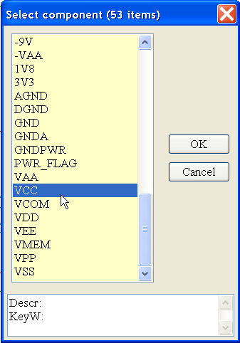
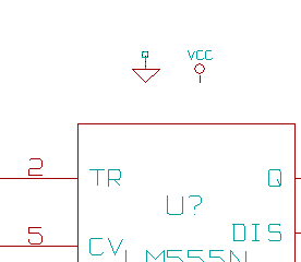
Add 9V and GND connectors.
Drawing Wires:
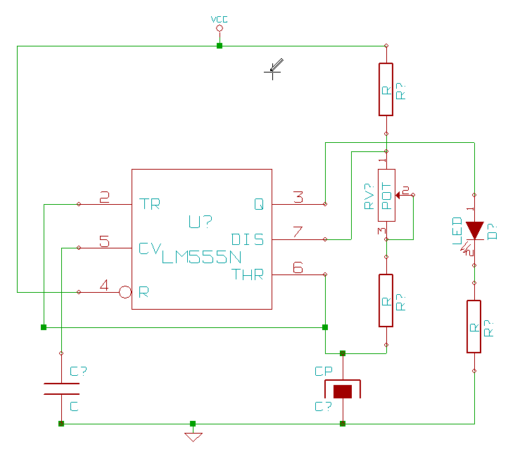
First, arrange the parts by hovering the mouse over them, and typing “M” or “R” to move or rotate.
Then select the Wire Drawing Tool. 
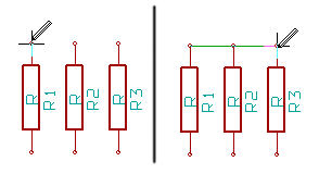
Note: you must start and end wires on the pins of components, it’s not enough that a wire visually connects with a component. For instance, if a wire is drawn between R1 and R3, R2 will not be connected.
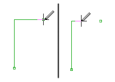
Tip: To erase part of a wire, draw back over it.
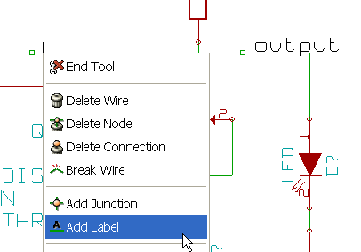
You can also connect nets and components by applying labels to wires. Just right click on a wire. Labels can be helpful for identifying traces when designing the pcb later on.
Where are the power and ground pins for the 555 chip?

Clock “Show Pins” to see the hidden power pins.
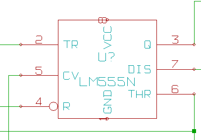
Now you can see pin 1 and 8. Because they are marked as being power pins in the component library, KiCad automatically connects these pins to wires that have power pins labeled VCC and GND. Note: If your select a different power pin, say 9V+, the implied connection won’t work. You would have to unhide the hidden power pins and manually connect them.
Annotating Components (numbering… R? –> R1, R2, C1, U1, etc.):
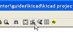
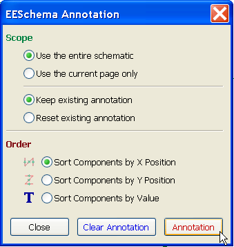
You need to number the components before moving on to the pcb layout. Click the Annotate Tool, set the params, and kicad automatically numbers all the components.
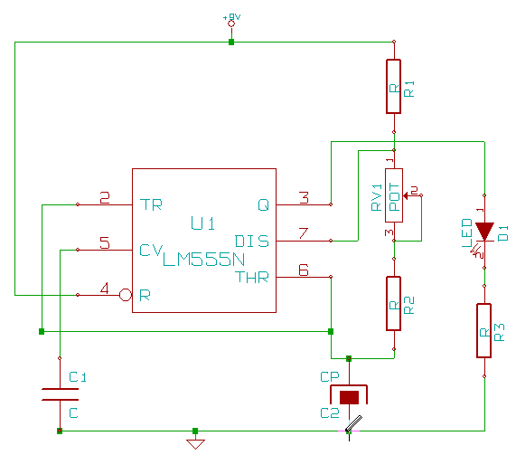
Adding values to components (10k, .01uF, etc.):
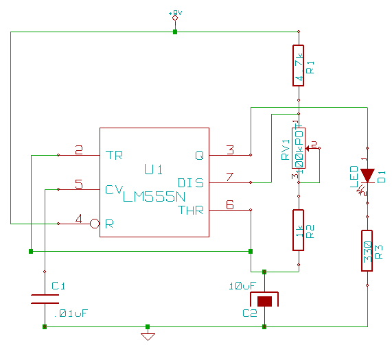
Just double click on the component to change its value.


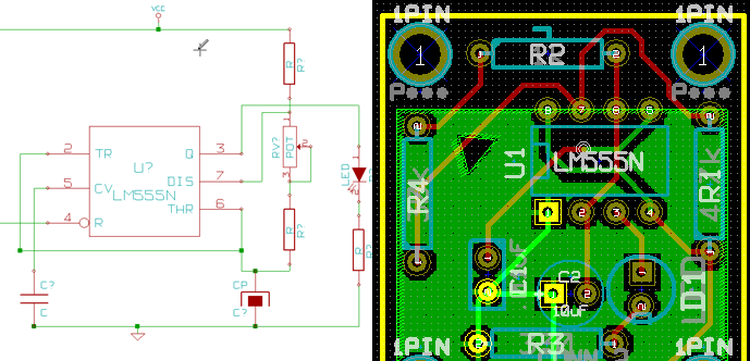
Feedback and corrections are greatly appreciated.
I can only get the first half of the video to play
sometimes the video can take a while to load—try reloading the page. A slightly lower resolution version of the how to solder video can be seen at YouTube.
great vid, very helpful!
Thank you for this video !!! Helped me out a lot !!! Really appreciate it !!
I have always had trouble getting good solder joints and to get solder to adhere on wire. Thank You for a very informative easy to understand Video and Narration.
cool!
sigh Remember people that lead is still by far the worse problem here. It takes about 8-15 micrograms (micro, not a mistake and I’ve thoroughly checked that) ingested per day to cause “lead poisoning” in a 6-year old. That means at least “special education” for Timmy, and it’s comparably bad for adults on a /kg basis. Just be smart and use lead-free. It’s a no-brainer for those who know the facts involved.
egads, I just watched the video. The way he is cleaning the solder tip, etc… When it’s sitting on a joint or used with prudence it’s one thing…. even intact solder will release lead oxide (a readily distributable powder) for a variety of reasons, and if you’re going to step on it, allow to oxidize under heat …. sand! Parts usually are pre-tinned with lead alloys. BAD IDEA…. look, using lead solder is a bad idea, okay. Don’t.
it’s illegal to use lead solder in plumbing, but the amount you’d get on your hands from doing these things here could be thousands of times what would leach out of solder joints into water you drink. True, I don’t know how much gets ingested from what’s on your hands, table feet floor, but we clearly have a problem here. It would be most interesting to try an experiment with an appropriate amount of bitrex on the surface of all the solder, and see if you notice how you end up ingesting it eventually – that would demonstrate how you cannot keep the lead in one place if you use it like this.
The hobbyist should be the last to use lead solder, and yet many in industry have already stopped. I’m not talking about “the environment”, I’m talking about not harming yourself and your household. Just think for a second the sort of concentrations we’re talking about in a landfill vs. your house. If having lead around matters in a landfill, it should matter in your house. Why am I writing this, apparently with some ulterior motive? Because I’ve seen how bad lead is, and I don’t want to have to put up with somebody else’s mess. Lead is so hard to clean up and easy to not put down, it’s time to grow up and start being a bit more responsible about it.
I hardly object to it’s use in SLA batteries for instance, but this is not it’s place.
While it’s certainly a good idea to wash your hands after soldering with lead-based solder, I’m not convinced that there’s significant risk to using lead-based solder. Sure, ingesting small amounts can be harmful, but how likely is it that small amounts wil actually be ingested?
Lead-free solder has its risks, too….
This claims there is evidence that the fumes from lead-free solder are more harmful (just how much more harmful? not sure…)
The lead-free alternatives have environmental costs as well.
It would be interesting to find out just how much lead from hand-soldering becomes ingested on average. I suspect it’s not a harmful amount. Assembly line workers have been assembling equipment with lead-based solder for a couple decades now, and I haven’t been able to find any studies showing a harmful amount of ingestion, although there are many that discuss the asthma risks from the flux fumes. (see this OKi ad)
Some more food for thought: this
article claims that there have actually been no documented studies showing ground water contamination from lead in land-fills (the main impetus for RoHS and WEEE regulations). Apparently lead from electronics comprises less than 1% of lead used, the rest coming mainly from batteries and CRT monitors (although the disposal of these is much more controlled). Note, lead can in fact be leached from PCBs, so I’m definitely not arguing against the prudence of those regulations.
I’d be very grateful for links to studies showing documented cases of lead-poisoning from hand-soldering.
excellent video – clear and to the point – great work.
Thanks a million. That video is a huge help. Very well done.
@scott: I’d highly suggest you watch Manufactured Landscape which has nothing to do with this except for one part where he goes to villages in China known for recycling electronics and noticed that you can smell the heavy metals from miles away and that the government now has to deliver water by truck as the natural sources are all contaminated.
point taken 🙂 If you have a link to youtube that’d be great…
I wonder what all is being thrown into that particular village… a lot of lead is used in car batteries here in the States, but their recycling is very much controlled, so little battery lead ends up in land fills.
Sounds like that village missed out on China’s version of RoHS.
why pronounce it “sawder”? Took me ages to work out what he was on about.
same reason it’s spelled “could” and sounds like “kude”
Outstanding video! I will be building a kit soon, and I found the information in the film will be of great help. Thanks so very much.
Dick Williams KB3OMJ
A good tutorial. I’ve been soldering for over 20 years (professionally and hobbyist), but it’s always good to brush up on techniques.
thanks… we’d love to hear any critiques you have or better ways of doing things that you’ve picked up over the years.
In further answer to the March 12, 2008 question “why pronounce it “sawder”? Took me ages to work out what he was on about,” please note that the questioner is not a native American english speaker, but rather a United Kingdom native speaker, wherever he/she actually resides. The North American pronunciation of “solder” is indeed “sawder.” But I would also point out that the phrase “he was on about” is equally obscure on this continent. It is not used here, except by those trying to emulate usage in Great Britain and its commonwealth. I would suggest that the original poster not be so critical, particularly while revealing his own linguistic shortcomings and lack of exposure to the usages of English around the world. The other commentator was a bit more cryptic, if more humorous than I, when he said “same reason it’s spelled “could” and sounds like “kude”. And finally, no less a personage than Sir Winston Churchill said something to the effect that “the UK & USA were two countries divided by the same language.” It was a good joke when he said it, and all the more so because it was so true, both then and now.
Now on to more important things. After all that, I will add that I thought the video was very well done, and will recommend it to a number of people with whom I work who will profit a great deal by it. I have been occasionally soldering electronic components for over 55 years now, and while I can recognize both bad and good solder joints, I have not been able to convey that knowledge to those 1/3 my age in nearly so clear a form as this video. Good work, and many thanks.
thanks!
And now for something completely different.
The online etymological dictionary says:
https://www.etymonline.com/index.php?term=solder
As for the snippish comment about “could”:
https://www.etymonline.com/index.php?term=could
Great Video! I’m just starting to get into some of this for repairing/modding old video game systems, to make them into musical devices and this gives me hope that with time I can start to understand the process enough not to mess it up.
I just broke the piece of metal on my glasses that connects the two lenses together and I was wondering if that was something that would be able to be soldered? I also have a 1 year old that loves grabbing at them so I would assume lead based solder wire would not be a good idea, any advice?
Hey, does anyone know what solder and devices would be needed for a newbie to desolder and resolder the audio wires for a nintendo ds lite??
I need it for no other purpose than that
please post questions in our soldering forum
thanks!
wow everything you said not to do I’ve done so this video is GREATLY apprieciated thank you!!!
This must be the best Tut Vid i have seen online !!
Tip requires sanding as the solder alloys with the copper of the tip forming brass. Brass has different solderability (wettability + thermal conductivity) than original high copper tip. Section a tip and metallographically prepare and etch it and it is readily apparant we are dealing with two metallurgically distinct regions. Sanding (grinding) is the solution .. excessive tinning might be the problem (along with excessive heat) under no-load conditions.
Spock out!
Very good vid. I especially like how you show bad examples, as well as good – that’s missing from other training videos I’ve seen.
And thanks too for tempering the OMG-Lead-We’re-Gonna-Die hysteria. Good links and rational info provided on the subject. I searched once trying to find the vapor pressure of lead at soldering temperatures. No luck except for one paper that had measured it at higher temps and extrapolated the result to soldering temps, describing it as: ‘a really hard vacuum’. The only other thing I’ve found are reports of no elevated blood levels of lead in electronics workers after years of ‘exposure’.
I’ve also read of the poor children in the contaminated ‘recycling villages’ in China (and elsewhere). If they weren’t being exposed to the tiny bit of lead in electronics, they will certainly be exposed to the much greater amount of lead in CRT’s and batteries. It’s
alldone illegally anyway, and if it’s not lead it’ll be something else that’s toxic, illegal, and profitable, that someone will use to expolit people at that level in that type of society. Removing lead in electronics is “not” a solution to that problem.Thanks for the video. I’ve done a little electronics soldering here and there over the last 20 years or so, and I’ve honestly never really had a clue what I was doing. This video was much more helpful than reading about it in a book.
Thanks a lot, this was a great help, I had done larger scale stuff, like pipes, but that’s a total different ball game.
Very good, just one suggestion: speak a little slower. Thank you!
great tutorial for someone who knows nothing from soldering
Excellent guide! Very useful.
i hoped to see this video moths ago, i reallly did a mess in my pcb projects, so now that i know how soldering, i will try hard to make a better work, thanks a lot ^^
I have done NASA certified soldering, and you have shown excellent views of good and bad joints. We used soft erasers to clean board pads and componant leads. Gold pads were more difficult to achieve a good shiny flow.
Great video, it’s all more clear now 🙂 Thank you.
This is the best how to solder video I’ve seen yet, and I’ve been looking at many. You explained the technique as well as the chemistry behind the process, and had good repetitive video samples. I had never heard of the heat bridge and soldering from the opposite side of the wire. Thanks a billion!